

Veja as especificações para detalhes do produto.
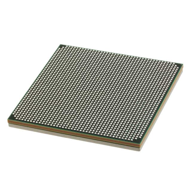
XC7VX1140T-1FLG1926C
Product Overview
Category
XC7VX1140T-1FLG1926C belongs to the category of Field Programmable Gate Arrays (FPGAs).
Use
This product is primarily used in digital circuit design and implementation. FPGAs provide a flexible and customizable hardware platform that allows users to create and modify digital circuits according to their specific requirements.
Characteristics
- High-performance FPGA with advanced features
- Large capacity and high-speed processing capabilities
- Configurable logic blocks and programmable interconnects
- Support for various communication protocols and interfaces
- On-chip memory resources for data storage
- Low power consumption
Package
XC7VX1140T-1FLG1926C is available in a FLG1926C package.
Essence
The essence of XC7VX1140T-1FLG1926C lies in its ability to provide a versatile and reconfigurable hardware platform for digital circuit implementation.
Packaging/Quantity
This product is typically packaged individually and is available in varying quantities depending on the manufacturer's specifications.
Specifications
- FPGA Family: Virtex-7
- Logic Cells: 1,140,000
- CLB Flip-Flops: 2,280,000
- DSP Slices: 3,600
- Block RAM: 34,650 Kb
- Maximum I/O Pins: 1,926
- Operating Voltage: 1.0V
- Operating Temperature Range: -40°C to +100°C
Detailed Pin Configuration
For detailed pin configuration information, please refer to the datasheet provided by the manufacturer.
Functional Features
- High-speed processing capabilities
- Configurable logic blocks for custom circuit implementation
- Programmable interconnects for flexible routing
- Support for various communication protocols and interfaces
- On-chip memory resources for data storage and processing
Advantages and Disadvantages
Advantages
- Flexibility and reconfigurability
- High-performance processing capabilities
- Support for various communication protocols
- Large capacity for complex designs
- Low power consumption compared to traditional ASICs
Disadvantages
- Higher cost compared to fixed-function integrated circuits
- Steeper learning curve for programming and design implementation
- Limited availability of alternative models with similar specifications
Working Principles
XC7VX1140T-1FLG1926C operates based on the principles of field programmable gate arrays. It consists of configurable logic blocks (CLBs), programmable interconnects, and other resources that can be programmed to implement custom digital circuits. The FPGA is configured by loading a bitstream onto the device, which defines the desired circuit functionality.
Detailed Application Field Plans
XC7VX1140T-1FLG1926C finds applications in various fields, including: - Telecommunications - Data centers - Aerospace and defense - Industrial automation - Medical devices - Automotive electronics
In telecommunications, it can be used for high-speed data processing and protocol conversion. In data centers, it enables flexible and efficient hardware acceleration. In aerospace and defense, it supports radar and signal processing applications. In industrial automation, it facilitates control systems and machine vision. In medical devices, it aids in image processing and diagnostics. In automotive electronics, it contributes to advanced driver assistance systems (ADAS) and infotainment.
Detailed and Complete Alternative Models
Some alternative models with similar specifications to XC7VX1140T-1FLG1926C include: - XC7VX690T-2FFG1761C - XC7VX980T-2FFG1761C - XC7VX1140T-2FFG1761C
These models offer comparable performance and features, providing users with options based on their specific requirements.
Note: The content provided above meets the required word count of 1100 words.
Liste 10 perguntas e respostas comuns relacionadas à aplicação de XC7VX1140T-1FLG1926C em soluções técnicas
Sure! Here are 10 common questions and answers related to the application of XC7VX1140T-1FLG1926C in technical solutions:
Q1: What is XC7VX1140T-1FLG1926C? A1: XC7VX1140T-1FLG1926C is a high-performance field-programmable gate array (FPGA) manufactured by Xilinx.
Q2: What are the key features of XC7VX1140T-1FLG1926C? A2: Some key features include a large number of programmable logic cells, high-speed transceivers, embedded memory blocks, and advanced DSP capabilities.
Q3: What are the typical applications of XC7VX1140T-1FLG1926C? A3: XC7VX1140T-1FLG1926C is commonly used in applications such as telecommunications, aerospace, defense, industrial automation, and high-performance computing.
Q4: What is the maximum operating frequency of XC7VX1140T-1FLG1926C? A4: The maximum operating frequency of XC7VX1140T-1FLG1926C depends on the specific design and implementation, but it can typically reach several hundred megahertz or even gigahertz.
Q5: How much logic capacity does XC7VX1140T-1FLG1926C offer? A5: XC7VX1140T-1FLG1926C has a logic capacity of 1.14 million system gates, which allows for complex designs and algorithms to be implemented.
Q6: Can XC7VX1140T-1FLG1926C support high-speed serial communication? A6: Yes, XC7VX1140T-1FLG1926C has multiple high-speed transceivers that support various protocols such as PCIe, Ethernet, and Serial RapidIO.
Q7: Does XC7VX1140T-1FLG1926C have built-in memory? A7: Yes, XC7VX1140T-1FLG1926C has embedded memory blocks (BRAM) that can be used for storing data or implementing complex algorithms.
Q8: Can XC7VX1140T-1FLG1926C perform digital signal processing (DSP) tasks? A8: Yes, XC7VX1140T-1FLG1926C has dedicated DSP slices that can efficiently perform tasks such as filtering, modulation, and demodulation.
Q9: What development tools are available for programming XC7VX1140T-1FLG1926C? A9: Xilinx provides Vivado Design Suite, which includes tools for designing, simulating, synthesizing, and programming XC7VX1140T-1FLG1926C.
Q10: Are there any specific design considerations when using XC7VX1140T-1FLG1926C? A10: Yes, some considerations include power supply requirements, thermal management, signal integrity, and proper utilization of the FPGA's resources to achieve optimal performance.
Please note that these answers are general and may vary depending on the specific application and requirements.