

Veja as especificações para detalhes do produto.
XC6SLX150T-2FGG900C
Product Overview
Category
XC6SLX150T-2FGG900C belongs to the category of Field Programmable Gate Arrays (FPGAs).
Use
This product is primarily used in digital logic circuits for various applications such as telecommunications, automotive, industrial automation, and consumer electronics.
Characteristics
- High-performance FPGA with advanced features
- Large capacity and high-speed processing capabilities
- Flexible and reprogrammable design
- Low power consumption
- Robust and reliable performance
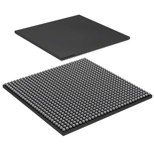
Package
XC6SLX150T-2FGG900C comes in a compact package that ensures easy integration into electronic systems. The package type is FG900, which refers to a Fine-Pitch Ball Grid Array (FBGA) package.
Essence
The essence of XC6SLX150T-2FGG900C lies in its ability to provide a customizable and versatile solution for complex digital circuit designs. It offers a wide range of features and functionalities that can be tailored to specific application requirements.
Packaging/Quantity
XC6SLX150T-2FGG900C is typically packaged in trays or reels, depending on the manufacturer's specifications. The quantity per package may vary, but it is commonly available in quantities suitable for both prototyping and production purposes.
Specifications
- FPGA Family: Spartan-6
- Logic Cells: 147,443
- Flip-Flops: 92,160
- Block RAM: 4,860 Kbits
- DSP Slices: 360
- Maximum Frequency: 550 MHz
- Operating Voltage: 1.2V
- I/O Voltage: 1.8V
- Package Type: FG900
Detailed Pin Configuration
The XC6SLX150T-2FGG900C has a total of 900 pins, each serving a specific purpose in the circuit design. The pin configuration is detailed in the product datasheet provided by the manufacturer.
Functional Features
- High-speed data processing capabilities
- Configurable logic blocks for custom circuit designs
- On-chip memory resources for efficient data storage
- Built-in digital signal processing (DSP) slices for complex algorithms
- Flexible I/O interfaces for seamless integration with external devices
- Clock management resources for precise timing control
Advantages and Disadvantages
Advantages
- Versatile and customizable design options
- High-performance processing capabilities
- Low power consumption
- Reliable and robust performance
- Wide range of application possibilities
Disadvantages
- Steep learning curve for beginners
- Limited availability of alternative models
- Higher cost compared to simpler logic devices
Working Principles
XC6SLX150T-2FGG900C operates based on the principles of reconfigurable logic. It consists of configurable logic blocks (CLBs), interconnect resources, and various other components that allow users to program and implement their desired digital circuits. The FPGA can be programmed using Hardware Description Languages (HDLs) such as VHDL or Verilog, enabling the creation of complex logic functions.
Detailed Application Field Plans
XC6SLX150T-2FGG900C finds applications in various fields, including:
- Telecommunications: Used in network routers, switches, and communication equipment for high-speed data processing.
- Automotive: Employed in automotive electronics for functions like engine control, driver assistance systems, and infotainment.
- Industrial Automation: Utilized in industrial control systems, robotics, and factory automation for real-time control and monitoring.
- Consumer Electronics: Integrated into devices like gaming consoles, high-definition televisions, and multimedia players for enhanced performance and functionality.
Detailed and Complete Alternative Models
While XC6SLX150T-2FGG900C offers a comprehensive set of features, there are alternative models available in the market that cater to different requirements. Some notable alternatives include:
- XC6SLX75T-3FGG484C: A lower-capacity FPGA suitable for cost-sensitive applications.
- XC7A35T-1CPG236C: A newer generation FPGA with enhanced performance and power efficiency.
- EP4CE115F29C7N: An FPGA from a different manufacturer offering similar capabilities.
These alternative models provide users with options based on their specific needs and budget constraints.
In conclusion, XC6SLX150T-2FGG900C is a high-performance FPGA that offers flexibility, reliability, and advanced features for various digital circuit applications. Its extensive pin configuration, functional features, and wide range of application fields make it a valuable component in the electronics industry.
Liste 10 perguntas e respostas comuns relacionadas à aplicação de XC6SLX150T-2FGG900C em soluções técnicas
Sure! Here are 10 common questions and answers related to the application of XC6SLX150T-2FGG900C in technical solutions:
Question: What is XC6SLX150T-2FGG900C?
Answer: XC6SLX150T-2FGG900C is a field-programmable gate array (FPGA) from Xilinx, which is commonly used in various technical solutions.Question: What are the key features of XC6SLX150T-2FGG900C?
Answer: Some key features of XC6SLX150T-2FGG900C include a high logic capacity, fast performance, low power consumption, and a wide range of I/O options.Question: In what applications can XC6SLX150T-2FGG900C be used?
Answer: XC6SLX150T-2FGG900C can be used in a wide range of applications such as telecommunications, industrial automation, aerospace, defense, and scientific research.Question: How can XC6SLX150T-2FGG900C be programmed?
Answer: XC6SLX150T-2FGG900C can be programmed using Xilinx's Vivado Design Suite or other compatible programming tools.Question: What is the maximum operating frequency of XC6SLX150T-2FGG900C?
Answer: The maximum operating frequency of XC6SLX150T-2FGG900C depends on the specific design and implementation, but it can typically reach several hundred megahertz.Question: Can XC6SLX150T-2FGG900C interface with other components or devices?
Answer: Yes, XC6SLX150T-2FGG900C supports various communication protocols and interfaces such as UART, SPI, I2C, Ethernet, and PCIe, allowing it to interface with other components or devices.Question: What is the power supply requirement for XC6SLX150T-2FGG900C?
Answer: XC6SLX150T-2FGG900C requires a 1.0V core voltage and a 2.5V or 3.3V auxiliary voltage for proper operation.Question: Can XC6SLX150T-2FGG900C be used in safety-critical applications?
Answer: Yes, XC6SLX150T-2FGG900C can be used in safety-critical applications, but additional measures may need to be taken to ensure reliability and fault tolerance.Question: Are there any development boards available for XC6SLX150T-2FGG900C?
Answer: Yes, Xilinx offers development boards specifically designed for XC6SLX150T-2FGG900C, which provide a convenient platform for prototyping and testing.Question: Where can I find more information about XC6SLX150T-2FGG900C?
Answer: You can find more detailed information about XC6SLX150T-2FGG900C in the official documentation provided by Xilinx, including datasheets, user guides, and application notes.