

Veja as especificações para detalhes do produto.
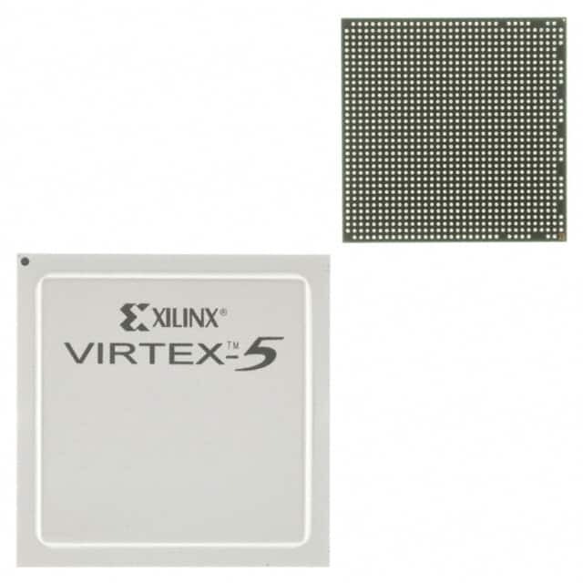
XC5VLX110-2FFG1153C
Product Overview
Category
The XC5VLX110-2FFG1153C belongs to the category of Field Programmable Gate Arrays (FPGAs).
Use
FPGAs are integrated circuits that can be programmed and reprogrammed to perform various digital functions. The XC5VLX110-2FFG1153C is specifically designed for high-performance applications.
Characteristics
- High-speed processing capabilities
- Large number of configurable logic blocks
- Flexible and reprogrammable design
- Low power consumption
- High reliability and durability
Package
The XC5VLX110-2FFG1153C comes in a Flip Chip FineLine BGA package.
Essence
The essence of the XC5VLX110-2FFG1153C lies in its ability to provide customizable digital functionality, allowing designers to implement complex systems on a single chip.
Packaging/Quantity
The XC5VLX110-2FFG1153C is typically packaged individually and is available in various quantities depending on the manufacturer's specifications.
Specifications
- Logic Cells: 110,000
- Block RAM: 4,800 Kbits
- DSP Slices: 352
- Maximum Frequency: 550 MHz
- I/O Pins: 1,153
- Operating Voltage: 1.2V
Detailed Pin Configuration
The XC5VLX110-2FFG1153C has a total of 1,153 I/O pins, each serving a specific purpose in the overall functionality of the FPGA. A detailed pin configuration diagram can be found in the product datasheet provided by the manufacturer.
Functional Features
- Configurable logic blocks allow for the implementation of complex digital circuits.
- High-speed processing capabilities enable efficient data manipulation.
- Integrated DSP slices provide hardware acceleration for signal processing tasks.
- Flexible I/O pins allow for easy interfacing with external devices.
- On-chip memory resources enable efficient data storage and retrieval.
Advantages
- Versatility: The XC5VLX110-2FFG1153C can be programmed to perform a wide range of functions, making it suitable for various applications.
- Reconfigurability: The FPGA's design allows for easy modification and adaptation to changing requirements.
- High Performance: The XC5VLX110-2FFG1153C offers fast processing speeds and ample resources for demanding applications.
- Power Efficiency: The low power consumption of the FPGA contributes to energy-efficient system designs.
- Reliability: FPGAs are known for their robustness and long lifespan.
Disadvantages
- Complexity: Designing and programming FPGAs can be challenging, requiring specialized knowledge and expertise.
- Cost: FPGAs tend to be more expensive compared to other integrated circuits due to their advanced capabilities.
- Limited Resources: Despite its high capacity, the XC5VLX110-2FFG1153C may not be sufficient for extremely complex designs.
Working Principles
The XC5VLX110-2FFG1153C operates based on the principles of configurable logic. It consists of an array of programmable logic blocks interconnected by configurable routing resources. By programming the interconnections and functionality of these blocks, designers can create custom digital circuits that perform specific tasks.
Detailed Application Field Plans
The XC5VLX110-2FFG1153C finds applications in various fields, including:
- Telecommunications: Used in network routers, switches, and base stations for high-speed data processing.
- Aerospace and Defense: Employed in radar systems, avionics, and military communication equipment.
- Industrial Automation: Utilized in control systems, robotics, and machine vision applications.
- Medical Devices: Integrated into medical imaging systems, patient monitoring devices, and diagnostic equipment.
- Automotive: Used in advanced driver-assistance systems (ADAS), infotainment systems, and engine control units.
Detailed and Complete Alternative Models
- XC7A100T-2FGG484C
- XC6SLX150-2FGG484C
- XC7K325T-2FFG900C
- XC6VLX240T-2FFG1156C
- XC7Z020-1CLG400C
These alternative models offer similar capabilities and can be considered as substitutes for the XC5VLX110-2FFG1153C depending on specific requirements.
In conclusion, the XC5VLX110-2FFG1153C is a high-performance FPGA that provides designers with the flexibility to implement complex digital circuits. Its versatile nature, coupled with its powerful processing capabilities, makes it suitable for a wide range of applications across various industries.
Liste 10 perguntas e respostas comuns relacionadas à aplicação de XC5VLX110-2FFG1153C em soluções técnicas
Sure! Here are 10 common questions and answers related to the application of XC5VLX110-2FFG1153C in technical solutions:
Question: What is XC5VLX110-2FFG1153C?
- Answer: XC5VLX110-2FFG1153C is a field-programmable gate array (FPGA) manufactured by Xilinx. It is part of the Virtex-5 family and offers high-performance logic and digital signal processing capabilities.Question: What are the key features of XC5VLX110-2FFG1153C?
- Answer: Some key features of XC5VLX110-2FFG1153C include 110,592 logic cells, 4,608 Kbits of block RAM, 128 DSP slices, and support for various I/O standards.Question: What are the typical applications of XC5VLX110-2FFG1153C?
- Answer: XC5VLX110-2FFG1153C is commonly used in applications such as telecommunications, aerospace, defense, industrial automation, and high-performance computing.Question: How can XC5VLX110-2FFG1153C be programmed?
- Answer: XC5VLX110-2FFG1153C can be programmed using Xilinx's Vivado Design Suite or ISE Design Suite software tools.Question: What is the maximum operating frequency of XC5VLX110-2FFG1153C?
- Answer: The maximum operating frequency of XC5VLX110-2FFG1153C depends on the specific design and implementation, but it can typically reach frequencies of several hundred megahertz.Question: Can XC5VLX110-2FFG1153C be used in a multi-FPGA system?
- Answer: Yes, XC5VLX110-2FFG1153C can be used in a multi-FPGA system by connecting multiple FPGAs together using high-speed serial interfaces such as PCIe or Ethernet.Question: What are the power requirements for XC5VLX110-2FFG1153C?
- Answer: The power requirements for XC5VLX110-2FFG1153C vary depending on the specific design and implementation, but it typically operates at voltages of 1.0V or 1.2V.Question: Does XC5VLX110-2FFG1153C support different I/O standards?
- Answer: Yes, XC5VLX110-2FFG1153C supports various I/O standards such as LVCMOS, LVTTL, LVDS, and differential signaling standards like SATA and PCIe.Question: Can XC5VLX110-2FFG1153C be reprogrammed after deployment?
- Answer: Yes, XC5VLX110-2FFG1153C is a field-programmable device, which means it can be reprogrammed even after it has been deployed in a system.Question: Are there any development boards available for XC5VLX110-2FFG1153C?
- Answer: Yes, Xilinx provides development boards like the ML505 and ML506 that are specifically designed to work with XC5VLX110-2FFG1153C and facilitate prototyping and development.
Please note that the answers provided here are general and may vary based on specific design requirements and implementation details.