

Veja as especificações para detalhes do produto.
XC3042L-8VQ100I
Product Overview
Category
XC3042L-8VQ100I belongs to the category of programmable logic devices (PLDs).
Use
This product is primarily used in digital circuit design and implementation. It offers a flexible and customizable solution for various applications.
Characteristics
- Programmable: The XC3042L-8VQ100I can be programmed to perform specific functions based on user requirements.
- High Integration: It integrates multiple logic gates, flip-flops, and other components into a single device.
- Versatile: This PLD can be used in a wide range of applications due to its programmability.
- Low Power Consumption: The XC3042L-8VQ100I is designed to operate efficiently with minimal power consumption.
Package
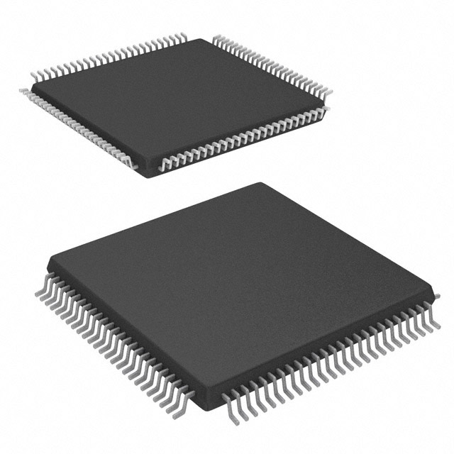
The XC3042L-8VQ100I comes in a VQFP (Very Thin Quad Flat Package) with 100 pins.
Essence
The essence of XC3042L-8VQ100I lies in its ability to provide a reconfigurable hardware platform that allows users to implement complex digital circuits.
Packaging/Quantity
The XC3042L-8VQ100I is typically packaged in reels or tubes, with each package containing a specified quantity of devices.
Specifications
- Logic Cells: 3042
- Operating Voltage: 3.3V
- Speed Grade: -8
- I/O Pins: 100
- Maximum Frequency: 100 MHz
- Configuration Memory: Non-volatile
Detailed Pin Configuration
The XC3042L-8VQ100I has a total of 100 pins, which are assigned different functions based on their configuration. The pin configuration is as follows:
(Pin Number) - (Pin Name) - (Function)
1 - VCCIO - Power Supply for I/O Buffers 2 - GND - Ground 3 - TCK - Test Clock Input 4 - TMS - Test Mode Select 5 - TDI - Test Data Input 6 - TDO - Test Data Output 7 - VCCINT - Internal Power Supply 8 - GND - Ground 9 - IO0 - General Purpose I/O Pin 0 10 - IO1 - General Purpose I/O Pin 1 ... 100 - IO99 - General Purpose I/O Pin 99
Functional Features
- Reconfigurability: The XC3042L-8VQ100I can be reprogrammed multiple times to adapt to changing design requirements.
- High-Speed Operation: It offers fast processing capabilities, making it suitable for applications that require quick response times.
- Flexible I/O Configuration: The device supports a variety of input and output configurations, allowing for versatile connectivity options.
- On-Chip Memory: The XC3042L-8VQ100I includes non-volatile memory for storing configuration data.
Advantages and Disadvantages
Advantages
- Flexibility: The programmable nature of the XC3042L-8VQ100I allows for easy customization and adaptation to different applications.
- Cost-Effective: By eliminating the need for custom-designed circuits, this PLD reduces development costs.
- Time-Saving: The reconfigurable nature of the device enables faster prototyping and iteration cycles.
Disadvantages
- Limited Complexity: While the XC3042L-8VQ100I is capable of implementing complex digital circuits, it may have limitations in handling extremely large designs.
- Learning Curve: Utilizing PLDs requires knowledge of hardware description languages and programming techniques, which may pose a learning curve for beginners.
Working Principles
The XC3042L-8VQ100I operates based on the principles of programmable logic. It consists of an array of configurable logic blocks (CLBs) interconnected by programmable routing resources. The device is programmed using a hardware description language (HDL) or a graphical design tool, which generates a configuration file. This file is then loaded into the PLD, configuring it to perform the desired logic functions.
Detailed Application Field Plans
The XC3042L-8VQ100I finds applications in various fields, including:
- Embedded Systems: It can be used to implement control and communication interfaces in embedded systems.
- Digital Signal Processing: The device enables the implementation of digital filters, signal generators, and other DSP algorithms.
- Industrial Automation: It can be utilized for controlling and monitoring industrial processes and machinery.
- Communication Systems: The XC3042L-8VQ100I can be employed in designing communication protocols and interfaces.
- Consumer Electronics: It finds use in consumer electronic devices such as gaming consoles, set-top boxes, and audio/video equipment.
Detailed and Complete Alternative Models
- XC9572XL-10VQG44C
- XC2S
Liste 10 perguntas e respostas comuns relacionadas à aplicação de XC3042L-8VQ100I em soluções técnicas
Sure! Here are 10 common questions and answers related to the application of XC3042L-8VQ100I in technical solutions:
Question: What is XC3042L-8VQ100I?
- Answer: XC3042L-8VQ100I is a specific model of Field-Programmable Gate Array (FPGA) manufactured by Xilinx.Question: What are the key features of XC3042L-8VQ100I?
- Answer: Some key features of XC3042L-8VQ100I include 3042 logic cells, 8 input/output banks, VQ100 package, and low power consumption.Question: What are the typical applications of XC3042L-8VQ100I?
- Answer: XC3042L-8VQ100I is commonly used in various technical solutions such as digital signal processing, embedded systems, telecommunications, industrial automation, and aerospace.Question: How can I program XC3042L-8VQ100I?
- Answer: XC3042L-8VQ100I can be programmed using Hardware Description Languages (HDLs) like VHDL or Verilog, or through Xilinx's Integrated Development Environment (IDE) called Vivado.Question: Can XC3042L-8VQ100I be reprogrammed after deployment?
- Answer: Yes, XC3042L-8VQ100I is a reprogrammable FPGA, allowing you to modify its functionality even after it has been deployed in a system.Question: What is the maximum operating frequency of XC3042L-8VQ100I?
- Answer: The maximum operating frequency of XC3042L-8VQ100I depends on the specific design and implementation, but it can typically reach frequencies of several hundred megahertz (MHz).Question: Can XC3042L-8VQ100I interface with other components or devices?
- Answer: Yes, XC3042L-8VQ100I supports various communication protocols such as SPI, I2C, UART, and GPIO, allowing it to interface with other components or devices in a system.Question: What is the power supply requirement for XC3042L-8VQ100I?
- Answer: XC3042L-8VQ100I operates at a voltage range of 3.3V, so it requires a stable 3.3V power supply for proper functioning.Question: Are there any development boards available for XC3042L-8VQ100I?
- Answer: Yes, Xilinx provides development boards like the Xilinx Spartan-3E Starter Kit that can be used for prototyping and testing designs using XC3042L-8VQ100I.Question: Where can I find technical documentation and support for XC3042L-8VQ100I?
- Answer: You can find technical documentation, datasheets, application notes, and support resources for XC3042L-8VQ100I on the official Xilinx website or by contacting their customer support.