

Veja as especificações para detalhes do produto.
XC2C256-7PQ208C
Product Overview
Category
XC2C256-7PQ208C belongs to the category of programmable logic devices (PLDs).
Use
This product is commonly used in digital circuit design and implementation. It provides a flexible and customizable solution for various applications.
Characteristics
- Programmable: The XC2C256-7PQ208C can be programmed to perform specific functions based on user requirements.
- High-density: It offers a large number of configurable logic blocks, allowing for complex designs.
- Low power consumption: The device is designed to operate efficiently with minimal power consumption.
- Fast operation: The XC2C256-7PQ208C provides high-speed performance, enabling rapid data processing.
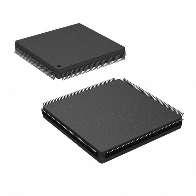
Package
The XC2C256-7PQ208C comes in a PQ208 package, which refers to a plastic quad flat pack with 208 pins.
Essence
The essence of XC2C256-7PQ208C lies in its ability to provide reconfigurable logic elements that can be programmed to perform specific tasks.
Packaging/Quantity
This product is typically packaged in reels or trays, depending on the manufacturer's specifications. The quantity per package may vary, but it is commonly available in quantities of 100 or more.
Specifications
- Device type: Programmable Logic Device (PLD)
- Family: XC2C
- Logic cells: 256
- Speed grade: -7
- Package: PQ208
- Operating voltage: 3.3V
- I/O standards: LVCMOS, LVTTL, HSTL, SSTL
- Maximum operating frequency: 200 MHz
- Programmable interconnects: 1,600
- User I/Os: 173
- RAM capacity: 4,608 bits
- JTAG interface: Yes
Detailed Pin Configuration
The XC2C256-7PQ208C has a total of 208 pins. The pin configuration is as follows:
(Pin number - Pin name) 1 - GND 2 - VCCIO0 3 - IOL1P0 4 - IOL1N0 5 - IOL2P0 6 - IOL2N0 ... 208 - VCC
Please refer to the product datasheet for the complete pin configuration details.
Functional Features
- Reconfigurable logic elements: The XC2C256-7PQ208C offers a large number of configurable logic blocks that can be programmed to implement various digital functions.
- Flexible I/O options: It provides multiple I/O standards, allowing compatibility with different voltage levels and signaling requirements.
- High-speed performance: The device operates at high frequencies, enabling efficient data processing and rapid response times.
- On-chip memory: The built-in RAM capacity allows for temporary storage of data during operation.
- JTAG interface: The JTAG interface facilitates programming and debugging of the device.
Advantages and Disadvantages
Advantages
- Flexibility: The XC2C256-7PQ208C's reprogrammable nature allows for easy modification and adaptation to changing design requirements.
- Cost-effective: By utilizing a single programmable device, it eliminates the need for multiple discrete components, reducing overall system costs.
- Time-saving: The ability to quickly modify the device's functionality significantly reduces development time compared to custom hardware solutions.
Disadvantages
- Complexity: Programming and configuring the XC2C256-7PQ208C requires expertise in digital circuit design and programming languages.
- Limited resources: The device has a finite number of logic cells and I/O pins, which may restrict the complexity and scale of designs.
Working Principles
The XC2C256-7PQ208C operates based on the principles of field-programmable gate arrays (FPGAs). It consists of configurable logic blocks interconnected through programmable interconnects. These logic blocks can be programmed to implement various digital functions by configuring their internal look-up tables and flip-flops.
During operation, the device receives input signals through its I/O pins, processes them using the configured logic elements, and produces the desired output signals. The JTAG interface allows for programming and debugging of the device, enabling the user to modify its functionality as needed.
Detailed Application Field Plans
The XC2C256-7PQ208C finds applications in various fields, including:
- Communications: It can be used in the development of communication systems, such as network routers and switches, to handle data processing and routing tasks efficiently.
- Industrial automation: The device is suitable for implementing control systems in industrial automation applications, enabling precise and flexible control over machinery and processes.
- Consumer electronics: It can be utilized in the design of consumer electronic devices, such as gaming consoles and multimedia players,
Liste 10 perguntas e respostas comuns relacionadas à aplicação de XC2C256-7PQ208C em soluções técnicas
Sure! Here are 10 common questions and answers related to the application of XC2C256-7PQ208C in technical solutions:
Question: What is XC2C256-7PQ208C?
- Answer: XC2C256-7PQ208C is a specific model of CoolRunner-II CPLD (Complex Programmable Logic Device) manufactured by Xilinx.Question: What is the purpose of using XC2C256-7PQ208C in technical solutions?
- Answer: XC2C256-7PQ208C is used for implementing digital logic functions, such as data processing, control systems, and interface protocols, in various electronic systems.Question: What are the key features of XC2C256-7PQ208C?
- Answer: Some key features of XC2C256-7PQ208C include 256 macrocells, 5V tolerant I/O pins, low power consumption, and reprogrammability.Question: How can XC2C256-7PQ208C be programmed?
- Answer: XC2C256-7PQ208C can be programmed using Xilinx's programming tools, such as iMPACT or Vivado, which allow users to configure the device with their desired logic functions.Question: What are the voltage requirements for XC2C256-7PQ208C?
- Answer: XC2C256-7PQ208C operates at a supply voltage range of 3.0V to 3.6V.Question: Can XC2C256-7PQ208C interface with other components or devices?
- Answer: Yes, XC2C256-7PQ208C can interface with other components or devices through its I/O pins, which can be configured as inputs or outputs.Question: What is the maximum frequency at which XC2C256-7PQ208C can operate?
- Answer: XC2C256-7PQ208C can operate at a maximum frequency of up to 200 MHz, depending on the design and implementation.Question: Can XC2C256-7PQ208C be used in high-reliability applications?
- Answer: Yes, XC2C256-7PQ208C is suitable for high-reliability applications as it has built-in features like error detection and correction, and robust design methodologies.Question: Are there any limitations or considerations when using XC2C256-7PQ208C?
- Answer: Some considerations include limited macrocell count, limited I/O pins, and the need for proper power supply decoupling and signal integrity measures.Question: Where can I find more information about XC2C256-7PQ208C and its application in technical solutions?
- Answer: You can refer to Xilinx's official documentation, datasheets, application notes, and online forums for more detailed information and specific application examples of XC2C256-7PQ208C.