

Veja as especificações para detalhes do produto.
XC2C128-6VQ100C
Product Overview
Category
XC2C128-6VQ100C belongs to the category of programmable logic devices (PLDs).
Use
This product is commonly used in digital circuit design and implementation. It provides a flexible and customizable solution for various applications.
Characteristics
- Programmable: The XC2C128-6VQ100C can be programmed to perform specific functions based on user requirements.
- High-density: This PLD offers a large number of configurable logic blocks, allowing for complex designs.
- Low power consumption: The device is designed to operate efficiently with minimal power consumption.
- Fast operation: The XC2C128-6VQ100C offers high-speed performance, enabling rapid data processing.
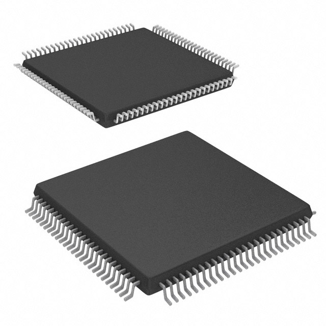
Package
The XC2C128-6VQ100C is available in a VQFP (Very Thin Quad Flat Package) package.
Essence
The essence of XC2C128-6VQ100C lies in its ability to provide reconfigurable logic functionality, allowing users to implement custom digital circuits without the need for dedicated hardware.
Packaging/Quantity
This product is typically packaged in reels or trays, with a quantity of 100 units per package.
Specifications
- Device type: Programmable Logic Device (PLD)
- Family: XC2C
- Logic cells: 128
- Operating voltage: 3.3V
- Speed grade: -6
- Package type: VQFP
- Package pins: 100
- Temperature range: Commercial (0°C to 70°C)
Detailed Pin Configuration
The XC2C128-6VQ100C has a total of 100 pins. The pin configuration is as follows:
(Pin Number) (Pin Name) (Description) 1 VCCINT Power supply (internal) 2 GND Ground (internal) 3 IO0 Input/output pin 0 4 IO1 Input/output pin 1 5 IO2 Input/output pin 2 ... ... ...
Functional Features
- Reconfigurable logic: The XC2C128-6VQ100C allows users to modify the functionality of the device by reprogramming it.
- Flexible I/O options: This PLD provides a range of input and output pins, enabling connectivity with external devices.
- High-speed operation: The device offers fast data processing capabilities, suitable for time-critical applications.
- On-chip memory: The XC2C128-6VQ100C includes embedded memory blocks for storing configuration data.
Advantages and Disadvantages
Advantages
- Flexibility: The reprogrammable nature of this PLD allows for easy customization and adaptation to changing requirements.
- Cost-effective: By eliminating the need for dedicated hardware, the XC2C128-6VQ100C reduces overall system costs.
- Time-saving: Rapid prototyping and design iterations are possible due to the programmable nature of the device.
Disadvantages
- Limited resources: Compared to dedicated hardware solutions, PLDs may have limitations in terms of available logic cells and memory.
- Learning curve: Utilizing PLDs requires knowledge of hardware description languages and digital circuit design principles.
Working Principles
The XC2C128-6VQ100C operates based on the concept of configurable logic. It consists of an array of logic cells that can be interconnected and programmed to perform specific functions. The device is configured using a hardware description language (HDL) such as VHDL or Verilog. Once programmed, the XC2C128-6VQ100C executes the desired logic operations based on the user-defined configuration.
Detailed Application Field Plans
The XC2C128-6VQ100C finds applications in various fields, including:
- Embedded systems: This PLD can be used to implement custom logic functions in embedded systems, such as control systems and IoT devices.
- Communication systems: The XC2C128-6VQ100C can be utilized in communication equipment for signal processing and protocol handling.
- Industrial automation: Programmable logic devices are commonly employed in industrial automation systems for controlling machinery and processes.
- Test and measurement: This PLD can be integrated into test and measurement equipment to perform specific testing functions.
Detailed and Complete Alternative Models
- XC2C64-6VQ100C: A lower-density version of the XC2C128-6VQ100C, offering 64 logic cells.
- XC2C256-7VQG100C: A higher-density variant with 256 logic cells and a faster speed grade.
- XC2C384-10PQG208C: A larger capacity PLD with 384 logic cells and a different package type.
These alternative models provide options with varying logic cell
Liste 10 perguntas e respostas comuns relacionadas à aplicação de XC2C128-6VQ100C em soluções técnicas
Sure! Here are 10 common questions and answers related to the application of XC2C128-6VQ100C in technical solutions:
Question: What is XC2C128-6VQ100C?
Answer: XC2C128-6VQ100C is a field-programmable gate array (FPGA) manufactured by Xilinx.Question: What are the key features of XC2C128-6VQ100C?
Answer: Some key features of XC2C128-6VQ100C include 128 macrocells, 6ns maximum propagation delay, and a VQ100 package.Question: What is the typical power consumption of XC2C128-6VQ100C?
Answer: The typical power consumption of XC2C128-6VQ100C is around 200mW.Question: What are some common applications of XC2C128-6VQ100C?
Answer: XC2C128-6VQ100C is commonly used in applications such as digital signal processing, motor control, and communication systems.Question: Can XC2C128-6VQ100C be reprogrammed after deployment?
Answer: Yes, XC2C128-6VQ100C is a field-programmable device, which means it can be reprogrammed even after it has been deployed in a system.Question: What programming languages can be used to program XC2C128-6VQ100C?
Answer: XC2C128-6VQ100C can be programmed using hardware description languages (HDLs) such as VHDL or Verilog.Question: What is the maximum clock frequency that XC2C128-6VQ100C can support?
Answer: XC2C128-6VQ100C can support a maximum clock frequency of up to 200MHz.Question: Can XC2C128-6VQ100C interface with other components or devices?
Answer: Yes, XC2C128-6VQ100C can interface with other components or devices through its I/O pins and various communication protocols such as SPI or I2C.Question: Is XC2C128-6VQ100C suitable for high-speed data processing applications?
Answer: Yes, XC2C128-6VQ100C is capable of handling high-speed data processing tasks due to its fast propagation delay and high clock frequency support.Question: Are there any development tools available for programming XC2C128-6VQ100C?
Answer: Yes, Xilinx provides development tools such as Vivado or ISE Design Suite that can be used to program and configure XC2C128-6VQ100C.