

Veja as especificações para detalhes do produto.
TC74VCX541FTEL
Basic Information Overview
- Category: Integrated Circuit (IC)
- Use: Logic Level Shifter
- Characteristics: High-speed, low-voltage, bidirectional buffer
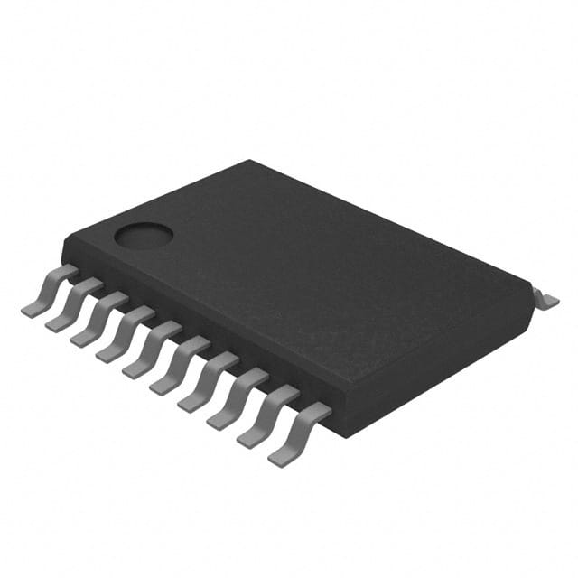
- Package: TSSOP-20
- Essence: Voltage level translation between different logic levels
- Packaging/Quantity: Tape and Reel, 2500 pieces per reel
Specifications
- Supply Voltage Range: 1.2V to 3.6V
- Input Voltage Range: GND to VCC
- Output Voltage Range: GND to VCC
- Maximum Operating Frequency: 200 MHz
- Number of Channels: 8
- Input/Output Type: Tri-State
Detailed Pin Configuration
The TC74VCX541FTEL has a total of 20 pins arranged as follows:
┌───┬───┐
   OE -|1  └─ 20|- VCC
  A1  -|2      19|- B1
  A2  -|3      18|- B2
  A3  -|4      17|- B3
  A4  -|5      16|- B4
  A5  -|6      15|- B5
  A6  -|7      14|- B6
  A7  -|8      13|- B7
  GND -|9      12|- B8
  A8  -|10     11|- OE#
       └───────┘
Functional Features
- Bidirectional voltage level shifting between different logic levels
- High-speed operation with minimal propagation delay
- Tri-state outputs for easy bus sharing
- Low power consumption
- ESD protection on all inputs and outputs
Advantages and Disadvantages
Advantages: - Wide supply voltage range allows compatibility with various systems - High-speed operation enables efficient data transfer - Tri-state outputs facilitate bus sharing in multi-device systems - ESD protection ensures robustness against electrostatic discharge
Disadvantages: - Limited number of channels (8) - Requires careful consideration of input and output voltage levels to prevent signal distortion
Working Principles
The TC74VCX541FTEL is a logic level shifter that allows bidirectional voltage translation between different logic levels. It operates by receiving input signals from one logic level and translating them to the desired logic level on the output side. The device utilizes a combination of MOSFETs and CMOS technology to achieve high-speed operation with minimal propagation delay.
Detailed Application Field Plans
The TC74VCX541FTEL is commonly used in various applications where voltage level translation is required. Some of the typical application fields include: - Communication systems - Data acquisition systems - Industrial automation - Consumer electronics - Automotive electronics
Detailed and Complete Alternative Models
- SN74LVC541A: Octal Buffer/Driver with 3-State Outputs
- MC74VHC541: Octal Buffer/Line Driver with 3-State Outputs
- CD74HCT541: High-Speed CMOS Logic Octal Buffer/Line Driver
These alternative models offer similar functionality and can be considered as substitutes for the TC74VCX541FTEL depending on specific requirements and availability.
In conclusion, the TC74VCX541FTEL is a high-speed, low-voltage logic level shifter integrated circuit. It provides bidirectional voltage level translation between different logic levels and is widely used in various applications. With its compact package and tri-state outputs, it offers convenience and flexibility in system design. However, designers should consider the limited number of channels and ensure proper handling of input and output voltage levels to avoid signal distortion.
Liste 10 perguntas e respostas comuns relacionadas à aplicação de TC74VCX541FTEL em soluções técnicas
Sure! Here are 10 common questions and answers related to the application of TC74VCX541FTEL in technical solutions:
Q: What is TC74VCX541FTEL? A: TC74VCX541FTEL is a voltage level translator IC (Integrated Circuit) that can be used to convert signals between different voltage levels.
Q: What is the operating voltage range of TC74VCX541FTEL? A: The operating voltage range of TC74VCX541FTEL is typically between 1.65V and 3.6V.
Q: Can TC74VCX541FTEL be used for bidirectional level translation? A: Yes, TC74VCX541FTEL supports bidirectional level translation, allowing signals to be translated from one voltage level to another in both directions.
Q: What is the maximum data rate supported by TC74VCX541FTEL? A: TC74VCX541FTEL can support data rates up to 200 Mbps (megabits per second).
Q: Is TC74VCX541FTEL suitable for use in battery-powered devices? A: Yes, TC74VCX541FTEL is designed to operate with low power consumption, making it suitable for use in battery-powered devices.
Q: Can TC74VCX541FTEL handle multiple voltage levels simultaneously? A: No, TC74VCX541FTEL is a single-supply voltage level translator and can only translate signals between two specific voltage levels.
Q: What is the input/output voltage threshold of TC74VCX541FTEL? A: The input/output voltage threshold of TC74VCX541FTEL is typically around half of the supply voltage.
Q: Does TC74VCX541FTEL have any built-in ESD protection? A: Yes, TC74VCX541FTEL is designed with built-in ESD (Electrostatic Discharge) protection to safeguard against static electricity damage.
Q: Can TC74VCX541FTEL be used in high-speed applications? A: Yes, TC74VCX541FTEL is suitable for high-speed applications due to its fast propagation delay and transition times.
Q: What package options are available for TC74VCX541FTEL? A: TC74VCX541FTEL is available in various package options, such as TSSOP (Thin Shrink Small Outline Package) and VFBGA (Very Fine Pitch Ball Grid Array).
Please note that the answers provided here are general and may vary depending on the specific datasheet and application requirements of TC74VCX541FTEL.