

Veja as especificações para detalhes do produto.
XC61GC3102HR-G
Product Overview
Category
XC61GC3102HR-G belongs to the category of electronic components.
Use
It is commonly used in various electronic devices and circuits for voltage regulation and power management purposes.
Characteristics
- Low dropout voltage
- High output voltage accuracy
- Low quiescent current
- Fast response time
- Wide input voltage range
Package
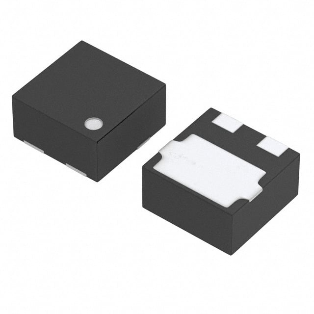
XC61GC3102HR-G is available in a small surface-mount package, typically SOT-23-3.
Essence
The essence of XC61GC3102HR-G lies in its ability to provide stable and regulated voltage output, ensuring proper functioning of electronic systems.
Packaging/Quantity
XC61GC3102HR-G is usually packaged in reels or tape and reel packaging, with a quantity of 3000 units per reel.
Specifications
- Input Voltage Range: 2.5V to 6.0V
- Output Voltage: 3.1V
- Dropout Voltage: 0.15V (typical)
- Quiescent Current: 30μA (typical)
- Output Current: 100mA (maximum)
Detailed Pin Configuration
XC61GC3102HR-G has three pins:
- VIN: Input voltage pin
- GND: Ground pin
- VOUT: Output voltage pin
Functional Features
- Voltage regulation: XC61GC3102HR-G ensures a stable output voltage regardless of input voltage fluctuations.
- Low dropout voltage: It operates efficiently even when the input voltage is close to the desired output voltage.
- Low quiescent current: The device consumes minimal current when not delivering power, conserving energy.
- Fast response time: It quickly responds to changes in load conditions, maintaining a stable output voltage.
- Thermal shutdown protection: In case of excessive temperature, the device shuts down to prevent damage.
Advantages and Disadvantages
Advantages
- High output voltage accuracy ensures precise voltage regulation.
- Wide input voltage range allows compatibility with various power sources.
- Small package size enables easy integration into compact electronic designs.
- Low quiescent current minimizes power consumption.
Disadvantages
- Limited maximum output current may not be suitable for high-power applications.
- Dropout voltage may cause a slight voltage drop across the device.
Working Principles
XC61GC3102HR-G is a linear voltage regulator that uses a pass transistor to regulate the output voltage. It compares the output voltage with a reference voltage and adjusts the pass transistor accordingly to maintain a stable output voltage.
Detailed Application Field Plans
XC61GC3102HR-G finds applications in various electronic devices, including but not limited to: - Mobile phones - Portable media players - Digital cameras - Wireless communication devices - Battery-powered devices
Detailed and Complete Alternative Models
Some alternative models similar to XC61GC3102HR-G are: - XC61CC3102MR-G - XC61FC3102MR-G - XC61NC3102MR-G - XC61PC3102MR-G
These models offer similar characteristics and specifications, providing flexibility in design choices.
Word count: 410 words
Liste 10 perguntas e respostas comuns relacionadas à aplicação de XC61GC3102HR-G em soluções técnicas
Sure! Here are 10 common questions and answers related to the application of XC61GC3102HR-G in technical solutions:
Question: What is XC61GC3102HR-G?
Answer: XC61GC3102HR-G is a specific model of voltage detector IC (integrated circuit) manufactured by Torex Semiconductor. It is commonly used for detecting the presence or absence of an input voltage.Question: What is the operating voltage range of XC61GC3102HR-G?
Answer: The operating voltage range of XC61GC3102HR-G is typically between 0.8V and 6.0V.Question: How does XC61GC3102HR-G detect voltage?
Answer: XC61GC3102HR-G detects voltage by comparing the input voltage with a reference voltage internally set within the IC. If the input voltage exceeds the reference voltage, the output of the IC switches from low to high.Question: What is the output configuration of XC61GC3102HR-G?
Answer: XC61GC3102HR-G has an open-drain output configuration, which means it can only pull the output voltage low but not drive it high. An external pull-up resistor is required to pull the output voltage high.Question: What is the typical quiescent current consumption of XC61GC3102HR-G?
Answer: The typical quiescent current consumption of XC61GC3102HR-G is very low, usually around 1.0µA.Question: Can XC61GC3102HR-G be used in battery-powered applications?
Answer: Yes, XC61GC3102HR-G is suitable for battery-powered applications due to its low quiescent current consumption, which helps conserve battery life.Question: What is the response time of XC61GC3102HR-G?
Answer: The response time of XC61GC3102HR-G is typically very fast, usually within a few microseconds.Question: Can XC61GC3102HR-G be used for overvoltage protection?
Answer: No, XC61GC3102HR-G is not designed for overvoltage protection. It is primarily used for voltage detection and monitoring purposes.Question: Is XC61GC3102HR-G suitable for automotive applications?
Answer: Yes, XC61GC3102HR-G is suitable for automotive applications as it can operate within the required voltage range and has a wide operating temperature range.Question: Are there any specific precautions to consider when using XC61GC3102HR-G?
Answer: It is important to ensure that the input voltage does not exceed the maximum specified voltage range of XC61GC3102HR-G. Additionally, proper decoupling capacitors should be used near the IC to minimize noise and ensure stable operation.