

Veja as especificações para detalhes do produto.
XC6119C33ANR-G
Product Overview
Category
XC6119C33ANR-G belongs to the category of voltage regulators.
Use
It is commonly used for regulating voltage in electronic circuits.
Characteristics
- Voltage regulation capability
- Low dropout voltage
- High output current
- Thermal shutdown protection
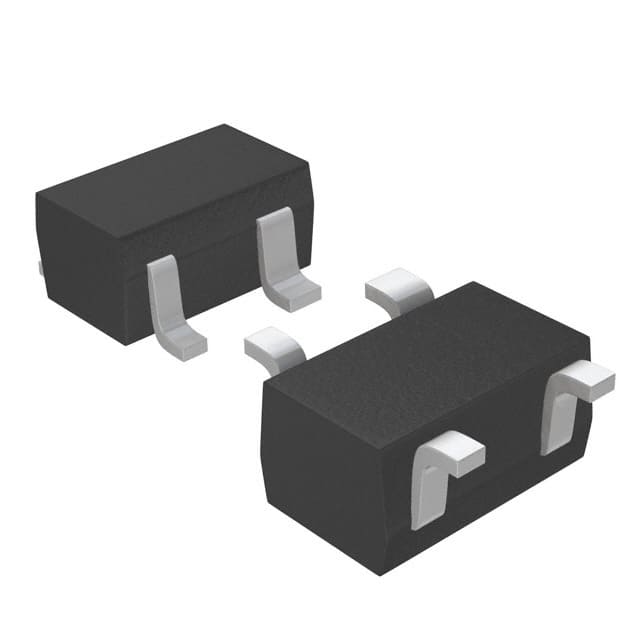
Package
XC6119C33ANR-G is available in a small surface-mount package.
Essence
The essence of XC6119C33ANR-G lies in its ability to regulate voltage efficiently and reliably.
Packaging/Quantity
This product is typically packaged in reels or tubes, with a quantity of 2500 units per reel/tube.
Specifications
- Input Voltage Range: 2.5V - 6.0V
- Output Voltage: 3.3V
- Output Current: Up to 500mA
- Dropout Voltage: 200mV (typical)
- Quiescent Current: 50μA (typical)
- Operating Temperature Range: -40°C to +85°C
Detailed Pin Configuration
XC6119C33ANR-G has the following pin configuration:
- VIN: Input voltage pin
- GND: Ground pin
- VOUT: Output voltage pin
- CE: Chip enable pin
Functional Features
- Voltage regulation: XC6119C33ANR-G ensures a stable output voltage of 3.3V regardless of input voltage fluctuations.
- Low dropout voltage: The device maintains a low voltage drop across it, minimizing power dissipation.
- High output current: It can deliver up to 500mA of current to power various components.
- Thermal shutdown protection: The regulator includes a thermal shutdown feature that protects it from overheating.
Advantages and Disadvantages
Advantages
- Efficient voltage regulation
- Low dropout voltage
- High output current capability
- Thermal shutdown protection ensures device safety
Disadvantages
- Limited input voltage range (2.5V - 6.0V)
- Quiescent current may be relatively high for some low-power applications
Working Principles
XC6119C33ANR-G operates based on the principle of a linear voltage regulator. It uses a feedback mechanism to maintain a constant output voltage, regardless of changes in the input voltage or load conditions. The internal circuitry compares the output voltage with a reference voltage and adjusts the pass transistor accordingly to regulate the output.
Detailed Application Field Plans
XC6119C33ANR-G finds applications in various electronic devices and systems, including but not limited to: - Battery-powered devices - Portable consumer electronics - Embedded systems - Industrial control systems - Automotive electronics
Detailed and Complete Alternative Models
Some alternative models that can be considered as alternatives to XC6119C33ANR-G are: - LM1117-3.3: A popular 3.3V linear voltage regulator with similar specifications. - LT1763-3.3: A low dropout 3.3V voltage regulator with excellent line and load regulation. - TPS79633: A high-performance 3.3V voltage regulator with low dropout voltage and low quiescent current.
These alternative models offer similar functionality and can be used as substitutes depending on specific requirements and availability.
Word count: 405 words
Liste 10 perguntas e respostas comuns relacionadas à aplicação de XC6119C33ANR-G em soluções técnicas
Sure! Here are 10 common questions and answers related to the application of XC6119C33ANR-G in technical solutions:
Q: What is XC6119C33ANR-G? A: XC6119C33ANR-G is a voltage detector IC (integrated circuit) that monitors the power supply voltage and provides a reset signal when the voltage drops below a certain threshold.
Q: What is the operating voltage range of XC6119C33ANR-G? A: The operating voltage range of XC6119C33ANR-G is typically between 0.8V and 6.0V.
Q: How does XC6119C33ANR-G help in technical solutions? A: XC6119C33ANR-G helps ensure stable operation of electronic devices by providing a reset signal when the power supply voltage falls below a specified level, preventing erratic behavior or data corruption.
Q: What is the output type of XC6119C33ANR-G? A: XC6119C33ANR-G has an open-drain output type, which means it can be connected to other devices with a pull-up resistor to achieve different logic levels.
Q: What is the typical reset threshold voltage of XC6119C33ANR-G? A: The typical reset threshold voltage of XC6119C33ANR-G is 3.3V, as indicated by the "C33" in its part number.
Q: Can XC6119C33ANR-G be used in battery-powered applications? A: Yes, XC6119C33ANR-G can be used in battery-powered applications as it operates within a wide voltage range and consumes very low quiescent current.
Q: Does XC6119C33ANR-G have any built-in delay for the reset signal? A: Yes, XC6119C33ANR-G has a built-in delay of approximately 200ms to ensure stable power supply before releasing the reset signal.
Q: Can XC6119C33ANR-G be used in automotive applications? A: Yes, XC6119C33ANR-G is suitable for automotive applications as it meets the necessary quality and reliability standards.
Q: What is the package type of XC6119C33ANR-G? A: XC6119C33ANR-G is available in a SOT-23-5 package, which is small and widely used in various electronic devices.
Q: Are there any application notes or reference designs available for XC6119C33ANR-G? A: Yes, the manufacturer of XC6119C33ANR-G provides application notes and reference designs that can help with the implementation of the IC in different technical solutions.
Please note that the answers provided here are general and may vary depending on specific datasheet information and application requirements.