

Veja as especificações para detalhes do produto.
SN75C3243PWR
Overview
Category: Integrated Circuit (IC)
Use: Signal Conditioning and Level Shifting
Characteristics: - Low voltage differential signaling (LVDS) driver and receiver - Designed for high-speed data transmission - Supports data rates up to 400 Mbps - Operates with a supply voltage range of 3V to 3.6V - Provides low power consumption
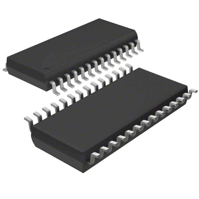
Package: TSSOP (Thin Shrink Small Outline Package)
Essence: SN75C3243PWR is an IC that facilitates signal conditioning and level shifting in high-speed data transmission applications.
Packaging/Quantity: The SN75C3243PWR is available in a TSSOP package and is typically sold in reels of 2500 units.
Specifications
- Supply Voltage Range: 3V to 3.6V
- Data Rate: Up to 400 Mbps
- Operating Temperature Range: -40°C to +85°C
- Input High Voltage (VIH): 2V to VCC + 0.3V
- Input Low Voltage (VIL): -0.3V to 0.8V
- Output High Voltage (VOH): VCC - 1.5V
- Output Low Voltage (VOL): 0.4V
Pin Configuration
The SN75C3243PWR has a total of 16 pins, which are assigned specific functions as follows:
- VCC - Power supply voltage
- GND - Ground
- A1 - LVDS input A
- B1 - LVDS input B
- Y1 - LVDS output Y
- Z1 - LVDS output Z
- A2 - LVDS input A
- B2 - LVDS input B
- Y2 - LVDS output Y
- Z2 - LVDS output Z
- A3 - LVDS input A
- B3 - LVDS input B
- Y3 - LVDS output Y
- Z3 - LVDS output Z
- A4 - LVDS input A
- B4 - LVDS input B
Functional Features
- Provides differential signaling for noise immunity and high-speed data transmission.
- Converts low voltage signals to LVDS levels for compatibility with LVDS receivers.
- Supports point-to-point and multipoint applications.
- Offers a wide supply voltage range for flexibility in various systems.
- Low power consumption enhances energy efficiency.
Advantages and Disadvantages
Advantages: - High-speed data transmission capability - Noise immunity due to differential signaling - Wide supply voltage range for compatibility with different systems - Low power consumption
Disadvantages: - Limited to LVDS interface applications - Requires additional components for complete signal conditioning
Working Principles
The SN75C3243PWR operates by receiving low voltage signals on the A1, B1, A2, B2, A3, B3, A4, and B4 pins. These signals are then converted to LVDS levels using internal circuitry. The converted LVDS signals are available at the Y1, Z1, Y2, Z2, Y3, Z3, Y4, and Z4 pins for further processing or transmission.
Detailed Application Field Plans
The SN75C3243PWR is commonly used in various applications that require signal conditioning and level shifting, such as:
- High-speed data communication systems
- Industrial automation and control systems
- Medical equipment
- Automotive electronics
- Test and measurement instruments
Detailed and Complete Alternative Models
- SN65LVDS3243PWR - Similar LVDS driver and receiver with extended temperature range (-40°C to +125°C).
- DS90LV032ATMTC/NOPB - Quad LVDS driver and receiver with higher data rate support (up to 1.5 Gbps).
- MAX9124ESE+T - LVDS driver and receiver with integrated ESD protection.
These alternative models offer similar functionality to the SN75C3243PWR and can be considered based on specific application requirements.
Word count: 524 words
Liste 10 perguntas e respostas comuns relacionadas à aplicação de SN75C3243PWR em soluções técnicas
Sure! Here are 10 common questions and answers related to the application of SN75C3243PWR in technical solutions:
Q: What is SN75C3243PWR? A: SN75C3243PWR is a quad differential line receiver IC commonly used for RS-485 communication applications.
Q: What is the operating voltage range of SN75C3243PWR? A: The operating voltage range of SN75C3243PWR is typically between 4.5V and 5.5V.
Q: Can SN75C3243PWR be used for half-duplex communication? A: Yes, SN75C3243PWR can be used for both half-duplex and full-duplex communication.
Q: What is the maximum data rate supported by SN75C3243PWR? A: SN75C3243PWR supports data rates up to 20 Mbps.
Q: Does SN75C3243PWR have built-in ESD protection? A: Yes, SN75C3243PWR has built-in ESD protection on the receiver inputs.
Q: Can SN75C3243PWR be used in industrial environments? A: Yes, SN75C3243PWR is designed to operate reliably in industrial environments with extended temperature ranges.
Q: How many receivers are there in SN75C3243PWR? A: SN75C3243PWR has four independent receivers.
Q: Is SN75C3243PWR compatible with TTL logic levels? A: Yes, SN75C3243PWR is compatible with both TTL and CMOS logic levels.
Q: Can SN75C3243PWR be used for long-distance communication? A: Yes, SN75C3243PWR is commonly used for long-distance communication due to its RS-485 compatibility.
Q: What is the package type of SN75C3243PWR? A: SN75C3243PWR is available in a small outline TSSOP-16 package.
Please note that these answers are general and may vary depending on specific application requirements.