

Veja as especificações para detalhes do produto.
SN74LVTH32374GKER
Product Overview
- Category: Integrated Circuit (IC)
- Use: Data storage and transfer
- Characteristics: High-speed, low-voltage, 32-bit D-type flip-flop with 3-state outputs
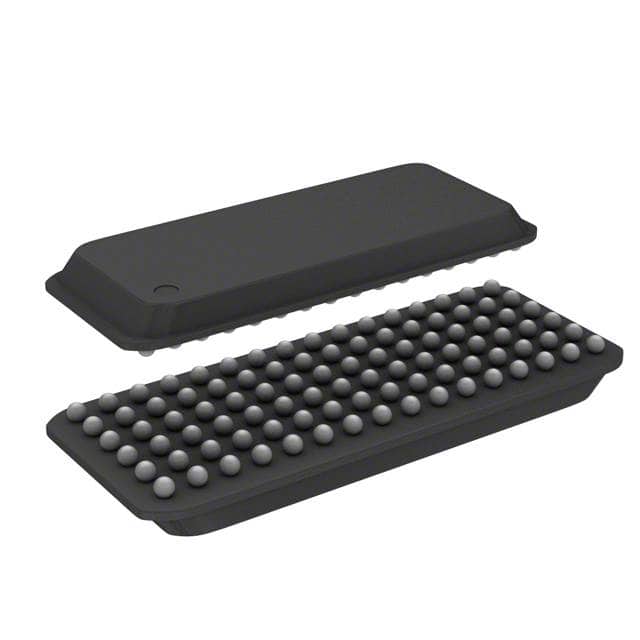
- Package: 48-pin TSSOP (Thin Shrink Small Outline Package)
- Essence: Flip-flop with 3-state outputs for efficient data storage and transfer
- Packaging/Quantity: Available in reels of 2500 units
Specifications
- Logic Family: LVTH
- Number of Bits: 32
- Supply Voltage Range: 2.7V to 3.6V
- High-Level Output Voltage: 2.4V (min), 3.3V (max)
- Low-Level Output Voltage: 0.4V (max)
- Input Voltage Range: -0.5V to 5.5V
- Operating Temperature Range: -40°C to 85°C
Detailed Pin Configuration
The SN74LVTH32374GKER has a total of 48 pins, which are assigned as follows:
- OE (Output Enable) 1
- Q0 (Output) 1
- D0 (Data) 1
- D1 (Data) 1
- Q1 (Output) 1
- GND (Ground)
- D2 (Data) 1
- D3 (Data) 1
- Q2 (Output) 1
- VCC (Power Supply)
- D4 (Data) 1
- D5 (Data) 1
- Q3 (Output) 1
- D6 (Data) 1
- D7 (Data) 1
- Q4 (Output) 1
- GND (Ground)
- D8 (Data) 1
- D9 (Data) 1
- Q5 (Output) 1
- VCC (Power Supply)
- D10 (Data) 1
- D11 (Data) 1
- Q6 (Output) 1
- D12 (Data) 1
- D13 (Data) 1
- Q7 (Output) 1
- GND (Ground)
- D14 (Data) 1
- D15 (Data) 1
- Q8 (Output) 1
- VCC (Power Supply)
- D16 (Data) 1
- D17 (Data) 1
- Q9 (Output) 1
- GND (Ground)
- D18 (Data) 1
- D19 (Data) 1
- Q10 (Output) 1
- VCC (Power Supply)
- D20 (Data) 1
- D21 (Data) 1
- Q11 (Output) 1
- D22 (Data) 1
- D23 (Data) 1
- Q12 (Output) 1
- GND (Ground)
- OE (Output Enable) 2
Functional Features
- High-speed operation: The SN74LVTH32374GKER is designed to operate at high speeds, making it suitable for applications that require fast data storage and transfer.
- Low-voltage operation: With a supply voltage range of 2.7V to 3.6V, this IC is compatible with low-power systems and can help reduce overall power consumption.
- 3-state outputs: The 3-state outputs allow multiple devices to share a common bus, enabling efficient data transfer and reducing the number of required pins.
Advantages and Disadvantages
Advantages: - High-speed operation enables quick data storage and transfer. - Low-voltage operation reduces power consumption. - 3-state outputs facilitate efficient data sharing.
Disadvantages: - Limited to 32-bit data storage and transfer. - Requires careful handling due to its small package size.
Working Principles
The SN74LVTH32374GKER is based on D-type flip-flop circuitry. It stores and transfers data using positive-edge-triggered clock inputs. When the clock signal transitions from low to high, the input data is latched and stored in the flip-flop. The stored data can then be outputted through the 3-state outputs when the output enable signal is active.
Detailed Application Field Plans
The SN74LVTH32374GKER is commonly used in various applications that require efficient data storage and transfer, such as:
- Microprocessors and microcontrollers
- Communication systems
- Data acquisition systems
Liste 10 perguntas e respostas comuns relacionadas à aplicação de SN74LVTH32374GKER em soluções técnicas
Sure! Here are 10 common questions and answers related to the application of SN74LVTH32374GKER:
Question: What is SN74LVTH32374GKER?
- Answer: SN74LVTH32374GKER is a 32-bit D-type flip-flop with 3-state outputs, designed for low-voltage (LV) and high-speed operation.Question: What is the operating voltage range of SN74LVTH32374GKER?
- Answer: SN74LVTH32374GKER operates within a voltage range of 2.7V to 3.6V.Question: What is the maximum data transfer rate supported by SN74LVTH32374GKER?
- Answer: SN74LVTH32374GKER supports a maximum data transfer rate of 400 Mbps.Question: Can SN74LVTH32374GKER be used in both input and output applications?
- Answer: Yes, SN74LVTH32374GKER can be used as both an input and output device.Question: What is the purpose of the 3-state outputs in SN74LVTH32374GKER?
- Answer: The 3-state outputs allow multiple devices to share a common bus without interfering with each other.Question: How many flip-flops are there in SN74LVTH32374GKER?
- Answer: SN74LVTH32374GKER consists of 32 individual D-type flip-flops.Question: What is the typical propagation delay of SN74LVTH32374GKER?
- Answer: The typical propagation delay of SN74LVTH32374GKER is around 3.8 ns.Question: Can SN74LVTH32374GKER be used in high-speed applications?
- Answer: Yes, SN74LVTH32374GKER is designed for high-speed operation and can be used in such applications.Question: Does SN74LVTH32374GKER have any built-in protection features?
- Answer: Yes, SN74LVTH32374GKER has built-in ESD protection to prevent damage from electrostatic discharge.Question: What is the package type of SN74LVTH32374GKER?
- Answer: SN74LVTH32374GKER comes in a 48-pin TSSOP (Thin Shrink Small Outline Package) package.
Please note that these answers are general and may vary depending on the specific application and requirements.