

Veja as especificações para detalhes do produto.
SN74LVC821ANSR
Product Overview
Category
SN74LVC821ANSR belongs to the category of integrated circuits (ICs).
Use
This IC is commonly used in digital logic applications.
Characteristics
- Low-voltage CMOS technology
- High-speed operation
- Wide operating voltage range
- Low power consumption
Package
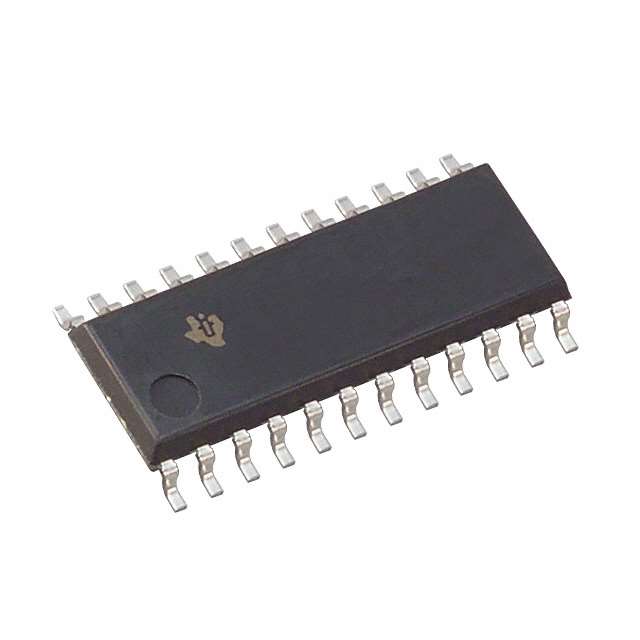
SN74LVC821ANSR is available in a small-outline package (SOIC) with 20 pins.
Essence
The essence of SN74LVC821ANSR lies in its ability to perform logical operations efficiently and reliably in various digital systems.
Packaging/Quantity
SN74LVC821ANSR is typically packaged in reels or tubes, with a quantity of 2500 units per reel/tube.
Specifications
- Supply Voltage: 1.65V to 5.5V
- Logic Family: LVC
- Number of Inputs: 10
- Number of Outputs: 10
- Operating Temperature Range: -40°C to +85°C
- Propagation Delay Time: 3.8 ns (typical)
- Output Current: ±24 mA
Detailed Pin Configuration
The pin configuration of SN74LVC821ANSR is as follows:
| Pin No. | Name | Description | |---------|------|-------------| | 1 | A1 | Input A1 | | 2 | B1 | Input B1 | | 3 | A2 | Input A2 | | 4 | B2 | Input B2 | | 5 | A3 | Input A3 | | 6 | B3 | Input B3 | | 7 | GND | Ground | | 8 | Y1 | Output Y1 | | 9 | Y2 | Output Y2 | | 10 | Y3 | Output Y3 | | 11-20 | NC | Not Connected |
Functional Features
- Performs logical AND operation on three sets of inputs (A1, B1), (A2, B2), and (A3, B3)
- Provides three corresponding outputs (Y1, Y2, Y3) based on the logical AND results
- High-speed operation allows for efficient processing of digital signals
- Wide operating voltage range enables compatibility with various systems
- Low power consumption ensures energy efficiency
Advantages and Disadvantages
Advantages
- High-speed operation enhances overall system performance
- Wide operating voltage range increases versatility
- Low power consumption reduces energy usage
- Compact package size facilitates integration into space-constrained designs
Disadvantages
- Limited number of inputs and outputs restricts the complexity of logic operations
- Propagation delay time may affect timing-sensitive applications
Working Principles
SN74LVC821ANSR operates based on the principles of digital logic. It performs logical AND operations on three sets of input signals and generates corresponding output signals based on the logical results. The IC utilizes low-voltage CMOS technology to achieve high-speed operation while maintaining low power consumption.
Detailed Application Field Plans
SN74LVC821ANSR finds applications in various digital systems, including but not limited to: - Microcontrollers - Data communication systems - Industrial automation - Consumer electronics - Automotive electronics
Detailed and Complete Alternative Models
Some alternative models that can be considered as alternatives to SN74LVC821ANSR are: - SN74LVC821ADGVR - SN74LVC821APW - SN74LVC821ARGYR - SN74LVC821APWRG4
These alternative models offer similar functionality and characteristics, providing flexibility in choosing the most suitable IC for specific applications.
In conclusion, SN74LVC821ANSR is a versatile integrated circuit that offers high-speed operation, low power consumption, and wide operating voltage range. Its logical AND functionality makes it suitable for various digital systems, and it can be easily integrated into different designs.
Liste 10 perguntas e respostas comuns relacionadas à aplicação de SN74LVC821ANSR em soluções técnicas
Sure! Here are 10 common questions and answers related to the application of SN74LVC821ANSR in technical solutions:
Q: What is SN74LVC821ANSR? A: SN74LVC821ANSR is a specific type of integrated circuit (IC) that functions as an 8-bit flip-flop with 3-state outputs.
Q: What are the typical applications of SN74LVC821ANSR? A: SN74LVC821ANSR is commonly used in digital systems for data storage, synchronization, and signal routing purposes.
Q: What is the operating voltage range of SN74LVC821ANSR? A: SN74LVC821ANSR operates within a voltage range of 1.65V to 5.5V.
Q: How many flip-flops are there in SN74LVC821ANSR? A: SN74LVC821ANSR consists of 8 individual flip-flops, each capable of storing one bit of data.
Q: Can SN74LVC821ANSR be cascaded to create larger storage capacities? A: Yes, multiple SN74LVC821ANSR ICs can be cascaded together to increase the overall storage capacity.
Q: What is the maximum clock frequency supported by SN74LVC821ANSR? A: SN74LVC821ANSR can operate at clock frequencies up to 100 MHz.
Q: Does SN74LVC821ANSR have any built-in output enable functionality? A: Yes, SN74LVC821ANSR has an active-low output enable pin (OE) that allows the outputs to be disabled when necessary.
Q: What is the power supply current consumption of SN74LVC821ANSR? A: The power supply current consumption of SN74LVC821ANSR varies depending on the operating conditions, but it typically ranges from a few microamps to a few milliamps.
Q: Can SN74LVC821ANSR tolerate overvoltage or undervoltage conditions? A: SN74LVC821ANSR has built-in protection mechanisms that allow it to tolerate limited overvoltage and undervoltage conditions without causing permanent damage.
Q: Are there any specific layout considerations for using SN74LVC821ANSR in a PCB design? A: Yes, it is recommended to follow the manufacturer's guidelines for proper decoupling capacitor placement and signal routing to minimize noise and ensure reliable operation.
Please note that these answers are general and may vary depending on the specific application and requirements. It is always advisable to refer to the datasheet and consult with the manufacturer for detailed information.