

Veja as especificações para detalhes do produto.
SN74LVC574ADGVR
Product Overview
- Category: Integrated Circuit (IC)
- Use: Flip-Flop
- Characteristics: Low-voltage, high-speed, octal D-type flip-flop with 3-state outputs
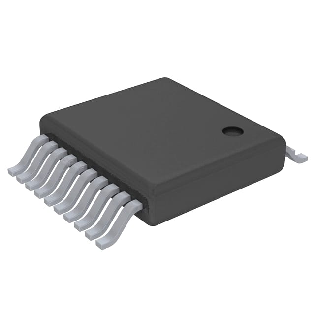
- Package: VSSOP (Very Small Outline Package)
- Essence: This IC is designed to store and transfer data in electronic circuits.
- Packaging/Quantity: Tape and Reel, 2500 pieces per reel
Specifications
- Supply Voltage Range: 1.65V to 3.6V
- High-Level Input Voltage: 2V to VCC + 0.5V
- Low-Level Input Voltage: -0.5V to 0.8V
- High-Level Output Voltage: 2.4V (min) at IOH = -12mA
- Low-Level Output Voltage: 0.4V (max) at IOL = 24mA
- Operating Temperature Range: -40°C to 85°C
Detailed Pin Configuration
The SN74LVC574ADGVR has a total of 20 pins. The pin configuration is as follows:
- GND (Ground)
- D0 (Data Input 0)
- D1 (Data Input 1)
- D2 (Data Input 2)
- D3 (Data Input 3)
- D4 (Data Input 4)
- D5 (Data Input 5)
- D6 (Data Input 6)
- D7 (Data Input 7)
- OE (Output Enable)
- CP (Clock Pulse)
- MR (Master Reset)
- Q0 (Flip-Flop Output 0)
- Q1 (Flip-Flop Output 1)
- Q2 (Flip-Flop Output 2)
- Q3 (Flip-Flop Output 3)
- Q4 (Flip-Flop Output 4)
- Q5 (Flip-Flop Output 5)
- Q6 (Flip-Flop Output 6)
- VCC (Supply Voltage)
Functional Features
- Octal D-type flip-flop with 3-state outputs
- High-speed operation, suitable for high-frequency applications
- Low-voltage operation, ideal for battery-powered devices
- 3-state outputs allow multiple ICs to be connected together without interference
- Master Reset (MR) input for clearing all flip-flops simultaneously
- Output Enable (OE) input for enabling/disabling the outputs
Advantages and Disadvantages
Advantages: - High-speed operation allows for efficient data transfer - Low-voltage operation reduces power consumption - 3-state outputs enable easy integration with other ICs - Compact VSSOP package saves board space
Disadvantages: - Limited temperature range (-40°C to 85°C) - Requires external clock pulse (CP) for proper operation
Working Principles
The SN74LVC574ADGVR is a positive-edge-triggered flip-flop. It stores data on the rising edge of the clock pulse (CP) input. The stored data is then available at the outputs (Q0-Q6) when the output enable (OE) signal is active. The master reset (MR) input can be used to clear all flip-flops simultaneously.
Detailed Application Field Plans
The SN74LVC574ADGVR is commonly used in various digital systems where data storage and transfer are required. Some application fields include:
- Microcontrollers and microprocessors
- Communication systems
- Data storage devices
- Industrial automation
- Automotive electronics
- Consumer electronics
Detailed and Complete Alternative Models
- SN74LVC574APWR
- SN74LVC574ADBR
- SN74LVC574ARGYR
- SN74LVC574ADW
These alternative models offer similar functionality and characteristics to the SN74LVC574ADGVR, providing options for different package types or quantities.
In conclusion, the SN74LVC574ADGVR is a versatile flip-flop IC that offers high-speed, low-voltage operation with 3-state outputs. Its compact package and wide range of applications make it a popular choice in various digital systems.
Liste 10 perguntas e respostas comuns relacionadas à aplicação de SN74LVC574ADGVR em soluções técnicas
Sure! Here are 10 common questions and answers related to the application of SN74LVC574ADGVR:
Q: What is the SN74LVC574ADGVR? A: The SN74LVC574ADGVR is a octal D-type flip-flop with 3-state outputs, commonly used in digital logic circuits.
Q: What is the operating voltage range of SN74LVC574ADGVR? A: The operating voltage range of SN74LVC574ADGVR is from 1.65V to 5.5V.
Q: What is the maximum clock frequency supported by SN74LVC574ADGVR? A: The maximum clock frequency supported by SN74LVC574ADGVR is typically around 100 MHz.
Q: How many flip-flops are there in SN74LVC574ADGVR? A: SN74LVC574ADGVR has 8 flip-flops, making it an octal (8-bit) flip-flop.
Q: What are the 3-state outputs in SN74LVC574ADGVR used for? A: The 3-state outputs allow multiple devices to share a common bus without interfering with each other.
Q: Can SN74LVC574ADGVR be used in both synchronous and asynchronous applications? A: Yes, SN74LVC574ADGVR can be used in both synchronous and asynchronous applications.
Q: What is the power supply current consumption of SN74LVC574ADGVR? A: The power supply current consumption of SN74LVC574ADGVR varies depending on the operating conditions, but it is typically low.
Q: Does SN74LVC574ADGVR have any built-in protection features? A: Yes, SN74LVC574ADGVR has built-in protection features like overvoltage and undervoltage lockout.
Q: Can SN74LVC574ADGVR be used in high-speed data transfer applications? A: Yes, SN74LVC574ADGVR is suitable for high-speed data transfer applications due to its fast propagation delay.
Q: What package options are available for SN74LVC574ADGVR? A: SN74LVC574ADGVR is available in various package options, such as TSSOP, VQFN, and SOIC.
Please note that the answers provided here are general and may vary depending on the specific datasheet and application requirements.