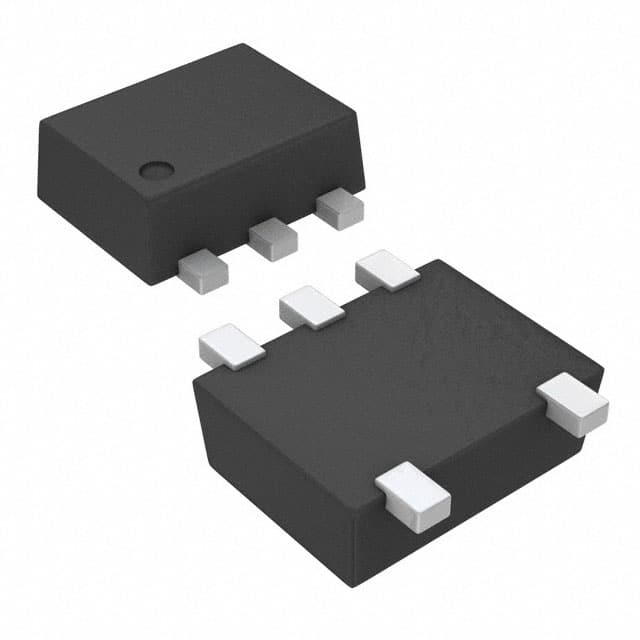
Veja as especificações para detalhes do produto.

SN74LVC1G126DRLR
Product Overview
- Category: Integrated Circuit (IC)
- Use: Logic Gate Buffer/Driver
- Characteristics: Single gate, low-voltage, high-speed, non-inverting buffer/driver
- Package: SOT-23-5
- Essence: Provides voltage level shifting and signal amplification for digital circuits
- Packaging/Quantity: Tape and Reel, 3000 units per reel
Specifications
- Supply Voltage Range: 1.65V to 5.5V
- High-Level Input Voltage: 0.7 x VCC
- Low-Level Input Voltage: 0.3 x VCC
- High-Level Output Voltage: 0.9 x VCC
- Low-Level Output Voltage: 0.1 x VCC
- Maximum Operating Frequency: 100 MHz
- Propagation Delay: 4.2 ns (typical)
Detailed Pin Configuration
The SN74LVC1G126DRLR has a total of 5 pins:
- GND (Ground): Connected to the ground reference of the circuit.
- A (Input): Accepts the input signal to be buffered or driven.
- OE (Output Enable): Controls the output state of the buffer/driver.
- Y (Output): Provides the buffered or driven output signal.
- VCC (Supply Voltage): Connected to the positive supply voltage of the circuit.
Functional Features
- Non-Inverting Buffer/Driver: The SN74LVC1G126DRLR provides a non-inverting function, meaning the output signal is the same as the input signal.
- High-Speed Operation: With a maximum operating frequency of 100 MHz, it can handle fast digital signals.
- Wide Supply Voltage Range: It can operate with a supply voltage ranging from 1.65V to 5.5V, making it compatible with various digital systems.
- Output Enable Control: The OE pin allows the user to enable or disable the output signal as needed.
Advantages and Disadvantages
Advantages: - Small Package Size: The SOT-23-5 package is compact, saving space on the circuit board. - Wide Supply Voltage Range: It can be used in a wide range of applications with different supply voltage levels. - High-Speed Operation: Suitable for high-frequency digital circuits.
Disadvantages: - Single Gate: Only one logic gate is included in the IC, limiting its functionality compared to multi-gate ICs. - Limited Output Current: The SN74LVC1G126DRLR has a maximum output current of 32 mA, which may not be sufficient for certain applications.
Working Principles
The SN74LVC1G126DRLR operates based on CMOS (Complementary Metal-Oxide-Semiconductor) technology. It consists of a single non-inverting buffer/driver gate that amplifies and buffers the input signal. When the OE pin is enabled, the input signal is passed through the gate and appears at the output pin. If the OE pin is disabled, the output is in a high-impedance state, effectively disconnecting it from the circuit.
Detailed Application Field Plans
The SN74LVC1G126DRLR is commonly used in various digital systems and applications, including:
- Microcontrollers: Provides level shifting and signal buffering for interfacing with other digital components.
- Communication Systems: Used in signal conditioning and amplification stages.
- Industrial Automation: Enables voltage level translation between different subsystems.
- Consumer Electronics: Utilized in portable devices, such as smartphones and tablets, for signal amplification and buffering.
- Automotive Electronics: Supports voltage level shifting and signal driving in automotive control systems.
Detailed and Complete Alternative Models
- SN74LVC1G125DCKR: Similar to SN74LVC1G126DRLR but with a different package (SC-70-5).
- SN74LVC1G07DCKR: Provides an open-drain output instead of a buffered output.
- SN74LVC1G04DBVR: Offers an inverting function instead of non-inverting.
These alternative models provide similar functionality but may differ in package type, pin configuration, or additional features.
In conclusion, the SN74LVC1G126DRLR is a single gate logic buffer/driver IC that operates at low voltage and high speed. It provides voltage level shifting and signal amplification for digital circuits. With its compact size and wide supply voltage range, it finds applications in various fields such as microcontrollers, communication systems, industrial automation, consumer electronics, and automotive electronics. While it has limitations like being a single gate IC and limited output current, there are alternative models available to suit specific requirements.
Liste 10 perguntas e respostas comuns relacionadas à aplicação de SN74LVC1G126DRLR em soluções técnicas
Sure! Here are 10 common questions and answers related to the application of SN74LVC1G126DRLR:
Q1: What is SN74LVC1G126DRLR? A1: SN74LVC1G126DRLR is a single bus buffer gate with 3-state output. It is commonly used in digital logic circuits for signal buffering and level shifting.
Q2: What is the operating voltage range of SN74LVC1G126DRLR? A2: The operating voltage range of SN74LVC1G126DRLR is from 1.65V to 5.5V.
Q3: What is the maximum output current of SN74LVC1G126DRLR? A3: The maximum output current of SN74LVC1G126DRLR is 32mA.
Q4: Can SN74LVC1G126DRLR be used as a level shifter? A4: Yes, SN74LVC1G126DRLR can be used as a level shifter to convert signals between different voltage levels.
Q5: How many inputs does SN74LVC1G126DRLR have? A5: SN74LVC1G126DRLR has one input.
Q6: How many outputs does SN74LVC1G126DRLR have? A6: SN74LVC1G126DRLR has one output.
Q7: What is the propagation delay of SN74LVC1G126DRLR? A7: The propagation delay of SN74LVC1G126DRLR is typically around 4.8ns.
Q8: Is SN74LVC1G126DRLR compatible with other logic families? A8: Yes, SN74LVC1G126DRLR is compatible with both CMOS and TTL logic families.
Q9: Can SN74LVC1G126DRLR be used in high-speed applications? A9: Yes, SN74LVC1G126DRLR is suitable for high-speed applications due to its fast switching speed.
Q10: What is the package type of SN74LVC1G126DRLR? A10: SN74LVC1G126DRLR is available in a small SOT-23-5 package.
Please note that these answers are general and may vary depending on specific datasheet specifications.

