

Veja as especificações para detalhes do produto.
SN74LVC1G125DRYR
Product Overview
- Category: Integrated Circuit (IC)
- Use: Buffer/Driver
- Characteristics: Single Gate, Non-Inverting, Tri-State Output
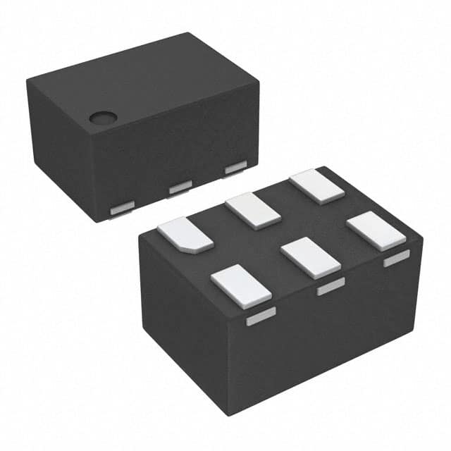
- Package: SOT-23-5
- Essence: Logic Level Shifter
- Packaging/Quantity: Tape and Reel, 3000 pieces per reel
Specifications
- Supply Voltage Range: 1.65V to 5.5V
- High-Level Input Voltage: 0.7 x Vcc
- Low-Level Input Voltage: 0.3 x Vcc
- High-Level Output Voltage: 0.9 x Vcc
- Low-Level Output Voltage: 0.1 x Vcc
- Maximum Operating Frequency: 100 MHz
- Maximum Propagation Delay: 4.8 ns
- Maximum Quiescent Current: 10 µA
Detailed Pin Configuration
The SN74LVC1G125DRYR has a total of 5 pins:
- GND (Ground): Connected to the ground reference of the circuit.
- OE (Output Enable): Controls the tri-state output buffer.
- A (Input): Data input pin.
- Y (Output): Buffered output pin.
- VCC (Supply Voltage): Connected to the positive supply voltage.
Functional Features
- Single gate buffer/driver with non-inverting logic.
- Tri-state output allows for high impedance state when disabled.
- Wide supply voltage range enables compatibility with various systems.
- Fast propagation delay ensures quick signal transmission.
- Low quiescent current minimizes power consumption.
Advantages and Disadvantages
Advantages: - Small form factor package saves board space. - Tri-state output provides flexibility in bus sharing applications. - Wide supply voltage range allows for compatibility with different voltage levels. - Fast propagation delay ensures efficient signal transmission.
Disadvantages: - Limited output current capability. - Single gate limits the number of inputs/outputs that can be handled.
Working Principles
The SN74LVC1G125DRYR is a logic level shifter that operates as a buffer/driver. It takes in a digital input signal and provides a buffered output signal with non-inverting logic. The tri-state output feature allows the device to enter a high impedance state when disabled, enabling multiple devices to share a common bus.
The IC operates within a wide supply voltage range, making it suitable for various applications. It has a fast propagation delay, ensuring quick signal transmission. The low quiescent current minimizes power consumption, making it energy-efficient.
Detailed Application Field Plans
The SN74LVC1G125DRYR is commonly used in the following applications:
- Microcontrollers: Level shifting between different voltage domains.
- Communication Systems: Signal buffering and level translation.
- Industrial Automation: Interface between sensors and control systems.
- Consumer Electronics: Logic level conversion in portable devices.
- Automotive Electronics: Signal conditioning and interfacing.
Detailed and Complete Alternative Models
- SN74LVC1G07DBVR: Single Buffer/Driver with Open-Drain Output
- SN74LVC1G04DCKR: Single Inverter Gate
- SN74LVC1G17DBVR: Single Schmitt-Trigger Buffer/Driver
- SN74LVC1G08DCKR: Single AND Gate
- SN74LVC1G86DBVR: Single XOR Gate
These alternative models offer similar functionality and characteristics, providing options for different design requirements.
Word count: 399 words
Liste 10 perguntas e respostas comuns relacionadas à aplicação de SN74LVC1G125DRYR em soluções técnicas
Sure! Here are 10 common questions and answers related to the application of SN74LVC1G125DRYR in technical solutions:
Q1: What is SN74LVC1G125DRYR? A1: SN74LVC1G125DRYR is a single bus buffer gate with 3-state output, designed for voltage level translation.
Q2: What is the operating voltage range of SN74LVC1G125DRYR? A2: The operating voltage range of SN74LVC1G125DRYR is from 1.65V to 5.5V.
Q3: What is the maximum output current of SN74LVC1G125DRYR? A3: The maximum output current of SN74LVC1G125DRYR is 32mA.
Q4: Can SN74LVC1G125DRYR be used as a level shifter? A4: Yes, SN74LVC1G125DRYR can be used as a level shifter to translate signals between different voltage levels.
Q5: What is the typical propagation delay of SN74LVC1G125DRYR? A5: The typical propagation delay of SN74LVC1G125DRYR is 4.3ns.
Q6: Is SN74LVC1G125DRYR suitable for high-speed applications? A6: Yes, SN74LVC1G125DRYR is suitable for high-speed applications due to its low propagation delay and high-speed operation.
Q7: Can SN74LVC1G125DRYR be used in bidirectional applications? A7: No, SN74LVC1G125DRYR is unidirectional and can only be used for one-way signal transmission.
Q8: What is the maximum operating frequency of SN74LVC1G125DRYR? A8: The maximum operating frequency of SN74LVC1G125DRYR is 500MHz.
Q9: Can SN74LVC1G125DRYR be used in automotive applications? A9: Yes, SN74LVC1G125DRYR is AEC-Q100 qualified and can be used in automotive applications.
Q10: Is SN74LVC1G125DRYR available in different package options? A10: Yes, SN74LVC1G125DRYR is available in various package options, such as SOT-23 and DSBGA.