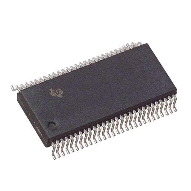
Veja as especificações para detalhes do produto.

SN74ALVCF162834LR
Product Overview
- Category: Integrated Circuit (IC)
- Use: Logic Level Translator
- Characteristics:
- Low voltage operation
- High-speed performance
- Bidirectional translation capability
- Wide operating voltage range
- Package: 56-pin BGA (Ball Grid Array)
- Essence: Logic level translation between different voltage domains
- Packaging/Quantity: Tape and Reel, 2500 units per reel
Specifications
- Supply Voltage Range: 1.2V to 3.6V
- Input Voltage Range (A Port): 0V to VCCA + 0.5V
- Input Voltage Range (B Port): 0V to VCCB + 0.5V
- Output Voltage Range (A Port): 0V to VCCA + 0.5V
- Output Voltage Range (B Port): 0V to VCCB + 0.5V
- Maximum Operating Frequency: 400 MHz
- Propagation Delay: 2.8 ns (typical)
- Output Drive Strength: ±24 mA
- ESD Protection: >2000V (Human Body Model)
Detailed Pin Configuration
The SN74ALVCF162834LR has a total of 56 pins. The pin configuration is as follows:
- A1
- A2
- A3
- A4
- A5
- A6
- A7
- A8
- A9
- A10
- A11
- A12
- A13
- A14
- A15
- A16
- GND
- OEAB
- VCCA
- VCCB
- B1
- B2
- B3
- B4
- B5
- B6
- B7
- B8
- B9
- B10
- B11
- B12
- B13
- B14
- B15
- B16
- GND
- OEBA
- VCCA
- VCCB
- DIR
- GND
- A17
- A18
- A19
- A20
- A21
- A22
- A23
- A24
- A25
- A26
- A27
- A28
- A29
- A30
Functional Features
- Bidirectional voltage level translation between two independent voltage domains (A and B)
- Automatic direction control based on the DIR pin
- Supports voltage translation from 1.2V to 3.6V
- High-speed operation with a maximum frequency of 400 MHz
- Low propagation delay for efficient signal transmission
- ESD protection for enhanced reliability
Advantages and Disadvantages
Advantages: - Wide operating voltage range allows compatibility with various systems - Bidirectional translation capability simplifies circuit design - High-speed performance enables fast data transfer - ESD protection ensures robustness against electrostatic discharge
Disadvantages: - Limited number of I/O pins (30 per voltage domain) - Relatively high power consumption compared to some alternative models - Sensitive to voltage fluctuations beyond specified ranges
Working Principles
The SN74ALVCF162834LR is designed to translate logic levels between two different voltage domains, typically used in mixed-voltage systems. It utilizes a bidirectional voltage level translation technique, allowing seamless communication between devices operating at different voltage levels.
The DIR pin controls the direction of translation. When DIR is set to logic low (0), the A port is connected to the B port, enabling translation from A to B. Conversely, when DIR is set to logic high (1), the B port is connected to the A port, facilitating translation from B to A.
The IC operates within a specified supply voltage range and provides ESD protection to safeguard against electrostatic discharge events. It offers high-speed performance with low propagation delay, ensuring efficient signal transmission between voltage domains.
Detailed Application Field Plans
The SN74ALVCF162834LR finds applications in various fields where logic level translation is required. Some potential application areas include:
- Mixed-voltage systems: Enables communication between devices operating at different voltage levels, such as microcontrollers, sensors, and display modules.
- Industrial automation: Facilitates data exchange between control systems and field devices with varying voltage requirements.
- Consumer electronics: Allows interoperability between components operating at different voltage levels, enhancing system integration and compatibility.
- Automotive electronics: Supports voltage
Liste 10 perguntas e respostas comuns relacionadas à aplicação de SN74ALVCF162834LR em soluções técnicas
Sure! Here are 10 common questions and answers related to the application of SN74ALVCF162834LR in technical solutions:
Q: What is SN74ALVCF162834LR? A: SN74ALVCF162834LR is a 16-bit universal bus driver with 3-state outputs, designed for low-voltage (1.65V to 3.6V) applications.
Q: What are the key features of SN74ALVCF162834LR? A: Some key features include wide voltage range, 3-state outputs, high-speed operation, and compatibility with various logic families.
Q: What is the maximum operating frequency of SN74ALVCF162834LR? A: The maximum operating frequency of SN74ALVCF162834LR is typically around 400 MHz.
Q: Can SN74ALVCF162834LR be used as a level shifter? A: Yes, SN74ALVCF162834LR can be used as a level shifter to interface between different voltage domains.
Q: How many output enable pins does SN74ALVCF162834LR have? A: SN74ALVCF162834LR has two output enable pins, which allow individual control of each output buffer.
Q: What is the power supply voltage range for SN74ALVCF162834LR? A: The power supply voltage range for SN74ALVCF162834LR is typically between 1.65V and 3.6V.
Q: Can SN74ALVCF162834LR drive capacitive loads? A: Yes, SN74ALVCF162834LR can drive moderate capacitive loads up to 50 pF.
Q: Is SN74ALVCF162834LR compatible with other logic families? A: Yes, SN74ALVCF162834LR is compatible with various logic families such as TTL, CMOS, and LVCMOS.
Q: What is the output current capability of SN74ALVCF162834LR? A: The output current capability of SN74ALVCF162834LR is typically around 24 mA.
Q: Can SN74ALVCF162834LR be used in automotive applications? A: Yes, SN74ALVCF162834LR is suitable for automotive applications as it meets the necessary standards and specifications.
Please note that these answers are general and may vary depending on specific datasheet information and application requirements.

