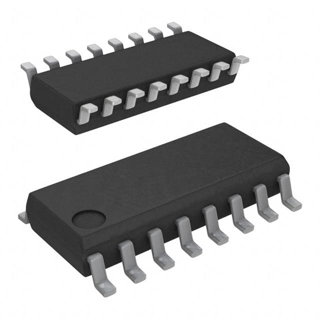
Veja as especificações para detalhes do produto.

CD74HCT283M96G4
Product Overview
- Category: Integrated Circuit
- Use: Arithmetic Logic Unit (ALU)
- Characteristics: High-Speed, CMOS Technology
- Package: SOIC-16
- Essence: 4-Bit Binary Full Adder
- Packaging/Quantity: Tape and Reel, 2500 units per reel
Specifications
- Supply Voltage: 2V to 6V
- Logic Family: HCT
- Number of Inputs: 8
- Number of Outputs: 4
- Propagation Delay: 13 ns
- Operating Temperature Range: -40°C to +85°C
Detailed Pin Configuration
The CD74HCT283M96G4 has a total of 16 pins. The pin configuration is as follows:
- A3 (Input)
- B3 (Input)
- C0 (Input)
- Carry-In (Input)
- Sum0 (Output)
- Carry-Out (Output)
- GND (Ground)
- A2 (Input)
- B2 (Input)
- A1 (Input)
- B1 (Input)
- A0 (Input)
- B0 (Input)
- C4 (Input)
- B4 (Input)
- VCC (Power)
Functional Features
- Performs binary addition of two 4-bit numbers
- Generates the sum output and carry-out signal
- Supports cascading for larger bit-width addition
- Utilizes high-speed CMOS technology for efficient operation
- Low power consumption
Advantages and Disadvantages
Advantages
- High-speed operation allows for quick arithmetic calculations
- Low power consumption makes it suitable for battery-powered devices
- Compact package size saves board space
- Wide operating temperature range enables usage in various environments
Disadvantages
- Limited to 4-bit addition, not suitable for larger bit-width calculations
- Requires external circuitry for carry-in and carry-out signals in cascaded applications
Working Principles
The CD74HCT283M96G4 is a 4-bit binary full adder that performs arithmetic addition of two 4-bit numbers. It utilizes CMOS technology, which ensures high-speed operation while maintaining low power consumption. The inputs A3-A0 and B3-B0 represent the four bits of the two numbers to be added. The carry-in (C0) input allows for cascading multiple adders to perform addition of larger bit-width numbers.
The output consists of the sum (Sum0-Sum3) and the carry-out (Carry-Out) signals. The sum outputs represent the binary representation of the addition result, while the carry-out signal indicates if there was a carry-over from the most significant bit. The CD74HCT283M96G4 operates within a wide temperature range, making it suitable for various applications.
Detailed Application Field Plans
The CD74HCT283M96G4 is commonly used in digital systems where arithmetic calculations are required. Some specific application fields include:
- Microcontrollers: Used in microcontroller units (MCUs) for performing arithmetic operations in embedded systems.
- Digital Signal Processing: Employed in digital signal processors (DSPs) for efficient number manipulation.
- Computer Arithmetic: Utilized in computer architecture for basic arithmetic calculations.
- Communication Systems: Integrated into communication devices for data processing and error correction.
- Industrial Automation: Incorporated in control systems for real-time calculations and data analysis.
Detailed and Complete Alternative Models
- SN74LS283: Similar 4-bit binary full adder with TTL logic family.
- CD74HC283: 4-bit binary full adder with high-speed CMOS technology.
- SN54LS283: Another TTL-based 4-bit binary full adder.
These alternative models provide similar functionality and can be used as replacements for the CD74HCT283M96G4 in various applications.
Word count: 498 words
Liste 10 perguntas e respostas comuns relacionadas à aplicação de CD74HCT283M96G4 em soluções técnicas
Sure! Here are 10 common questions and answers related to the application of CD74HCT283M96G4 in technical solutions:
Q: What is CD74HCT283M96G4? A: CD74HCT283M96G4 is a high-speed CMOS logic IC, specifically a 4-bit binary full adder with fast carry.
Q: What are the key features of CD74HCT283M96G4? A: Some key features include low power consumption, high-speed operation, compatibility with TTL inputs, and wide operating voltage range.
Q: How can CD74HCT283M96G4 be used in technical solutions? A: It can be used in various applications such as arithmetic operations, data processing, digital signal processing, and control systems.
Q: What is the maximum operating frequency of CD74HCT283M96G4? A: The maximum operating frequency is typically around 50 MHz.
Q: Can CD74HCT283M96G4 handle both positive and negative voltages? A: No, CD74HCT283M96G4 operates on positive supply voltages only.
Q: Is CD74HCT283M96G4 compatible with other logic families? A: Yes, CD74HCT283M96G4 is compatible with TTL (Transistor-Transistor Logic) inputs, making it versatile for integration with other logic devices.
Q: What is the power supply voltage range for CD74HCT283M96G4? A: The power supply voltage range is typically between 4.5V and 5.5V.
Q: Does CD74HCT283M96G4 have built-in protection against electrostatic discharge (ESD)? A: Yes, CD74HCT283M96G4 has built-in ESD protection to prevent damage during handling and operation.
Q: Can CD74HCT283M96G4 be used in high-temperature environments? A: Yes, CD74HCT283M96G4 is designed to operate reliably at elevated temperatures, typically up to 125°C.
Q: Are there any specific application notes or reference designs available for CD74HCT283M96G4? A: Yes, the manufacturer provides application notes and reference designs that can help in implementing CD74HCT283M96G4 in various technical solutions.
Please note that the answers provided here are general and may vary based on specific datasheets and manufacturer documentation.

