

Veja as especificações para detalhes do produto.
CD4097BNSR
Product Overview
Category
CD4097BNSR belongs to the category of integrated circuits (ICs).
Use
This product is commonly used in electronic circuits for signal processing and control applications.
Characteristics
- CD4097BNSR is a CMOS-based quad bilateral switch.
- It operates at a wide voltage range, typically from 3V to 18V.
- The device offers low power consumption and high noise immunity.
- It has a compact package, making it suitable for space-constrained designs.
Package
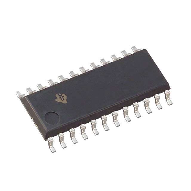
CD4097BNSR is available in a small outline package (SOIC) with 16 pins.
Essence
The essence of CD4097BNSR lies in its ability to control the flow of signals in electronic circuits, enabling various switching operations.
Packaging/Quantity
This product is typically sold in reels or tubes containing multiple units. The exact quantity may vary depending on the supplier.
Specifications
- Supply Voltage Range: 3V to 18V
- On-State Resistance: 125Ω (typical)
- Operating Temperature Range: -55°C to +125°C
- Input/Output Logic Level: CMOS/TTL compatible
Detailed Pin Configuration
The CD4097BNSR IC has 16 pins arranged as follows:
```
| | --|1 16|-- VDD --|2 15|-- INHIBIT --|3 14|-- A0 --|4 13|-- B0 --|5 12|-- C0 --|6 11|-- D0 --|7 10|-- D1 --|8 9|-- C1 |___________| ```
Functional Features
- Quad Bilateral Switch: CD4097BNSR consists of four independent bilateral switches, allowing multiple signal paths to be controlled simultaneously.
- High-Speed Operation: The device offers fast switching times, enabling efficient signal routing in time-critical applications.
- Low Power Consumption: CD4097BNSR is designed to minimize power consumption, making it suitable for battery-powered devices.
- Wide Voltage Range: It can operate within a wide voltage range, providing flexibility in various electronic systems.
Advantages and Disadvantages
Advantages
- Versatile functionality with four independent bilateral switches.
- Compact package size allows for space-efficient designs.
- Low power consumption extends battery life in portable devices.
- Wide operating voltage range provides compatibility with different systems.
Disadvantages
- Limited on-state resistance may introduce some signal attenuation.
- Not suitable for high-frequency applications due to inherent capacitance.
Working Principles
CD4097BNSR operates based on the principles of CMOS technology. When the control signals are applied to the appropriate pins, the internal switches connect or disconnect the input and output terminals, allowing or blocking the flow of signals.
Detailed Application Field Plans
CD4097BNSR finds applications in various fields, including:
- Audio Systems: Used for audio signal routing and mixing in audio mixers and amplifiers.
- Communication Systems: Employed in signal switching and routing circuits in telecommunication equipment.
- Industrial Control: Utilized for controlling signals in industrial automation systems.
- Test and Measurement: Integrated into test equipment for signal routing and multiplexing purposes.
Detailed and Complete Alternative Models
Some alternative models that offer similar functionality to CD4097BNSR include:
- CD4066BNSR: A quad bilateral switch with similar characteristics and pin configuration.
- DG403DJZ: Another quad bilateral switch with enhanced on-state resistance and lower power consumption.
- MAX4544EUT+: A high-speed quad bilateral switch suitable for applications requiring fast switching times.
These alternative models can be considered based on specific requirements and design constraints.
Word count: 520 words
Liste 10 perguntas e respostas comuns relacionadas à aplicação de CD4097BNSR em soluções técnicas
Sure! Here are 10 common questions and answers related to the application of CD4097BNSR in technical solutions:
Q: What is CD4097BNSR? A: CD4097BNSR is a CMOS analog multiplexer/demultiplexer integrated circuit (IC) that can be used for various signal routing applications.
Q: What is the operating voltage range of CD4097BNSR? A: The operating voltage range of CD4097BNSR is typically between 3V and 18V.
Q: How many channels does CD4097BNSR have? A: CD4097BNSR has 8 channels, which means it can route signals between 8 different inputs and outputs.
Q: Can CD4097BNSR handle both analog and digital signals? A: Yes, CD4097BNSR is designed to handle both analog and digital signals, making it versatile for various applications.
Q: What is the maximum frequency range supported by CD4097BNSR? A: CD4097BNSR can support frequencies up to several megahertz, depending on the specific application and conditions.
Q: Is CD4097BNSR suitable for bidirectional signal routing? A: No, CD4097BNSR is not bidirectional. It can only route signals from input to output or vice versa, but not simultaneously.
Q: Can CD4097BNSR be cascaded to increase the number of channels? A: Yes, multiple CD4097BNSR ICs can be cascaded together to increase the number of channels and expand the signal routing capabilities.
Q: What is the power consumption of CD4097BNSR? A: CD4097BNSR has low power consumption, typically in the range of a few milliwatts.
Q: Does CD4097BNSR have built-in protection features? A: Yes, CD4097BNSR includes built-in electrostatic discharge (ESD) protection to safeguard against damage during handling and operation.
Q: What are some common applications of CD4097BNSR? A: CD4097BNSR can be used in various technical solutions such as audio/video signal routing, data acquisition systems, test equipment, and communication devices.
Please note that these answers are general and may vary depending on the specific datasheet and application requirements of CD4097BNSR.