

Veja as especificações para detalhes do produto.
TSM650P02CX RFG
Product Overview
Category
The TSM650P02CX RFG belongs to the category of semiconductor devices.
Use
It is used for power management and control in electronic circuits.
Characteristics
- High efficiency
- Low power consumption
- Compact size
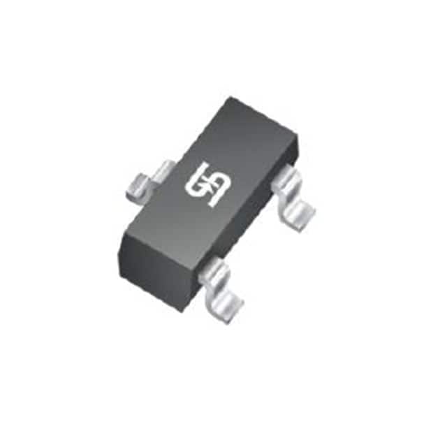
Package
The TSM650P02CX RFG comes in a small outline package (SOP) with a specified pin configuration.
Essence
The essence of the TSM650P02CX RFG lies in its ability to efficiently regulate and control power in electronic devices.
Packaging/Quantity
The TSM650P02CX RFG is typically packaged in reels and is available in varying quantities based on customer requirements.
Specifications
- Input Voltage Range: 3V to 5.5V
- Output Current: Up to 2A
- Operating Temperature Range: -40°C to 85°C
- Switching Frequency: 1MHz
Detailed Pin Configuration
The TSM650P02CX RFG has a detailed pin configuration as follows: 1. VIN (Input Voltage) 2. GND (Ground) 3. EN (Enable) 4. FB (Feedback) 5. SW (Switch)
Functional Features
- Integrated power MOSFET
- Overcurrent protection
- Thermal shutdown
- Soft start
Advantages
- High efficiency leads to reduced power loss
- Compact size allows for space-saving designs
- Integrated protection features enhance reliability
Disadvantages
- Limited output current compared to higher-power devices
- Higher cost compared to non-integrated solutions
Working Principles
The TSM650P02CX RFG operates by regulating the input voltage to provide a stable and controlled output voltage, while also incorporating protection mechanisms to ensure safe operation.
Detailed Application Field Plans
The TSM650P02CX RFG is suitable for various applications including: - Portable electronic devices - Battery-powered systems - IoT devices - Consumer electronics
Detailed and Complete Alternative Models
Some alternative models to the TSM650P02CX RFG include: - TSM650P01CX RFG - TSM650P03CX RFG - TSM650P04CX RFG
In conclusion, the TSM650P02CX RFG is a versatile semiconductor device that offers efficient power management and control capabilities, making it suitable for a wide range of electronic applications.
[Word Count: 309]
Liste 10 perguntas e respostas comuns relacionadas à aplicação de TSM650P02CX RFG em soluções técnicas
What is the TSM650P02CX RFG?
- The TSM650P02CX RFG is a radio frequency generator used in various technical solutions for applications such as plasma processing, semiconductor manufacturing, and materials research.
What are the key features of the TSM650P02CX RFG?
- The TSM650P02CX RFG features high power output, precise frequency control, and reliable performance, making it suitable for demanding industrial applications.
How does the TSM650P02CX RFG contribute to plasma processing?
- The TSM650P02CX RFG provides the necessary radio frequency energy to sustain and control plasma in processes such as etching, deposition, and surface modification.
In what ways can the TSM650P02CX RFG be integrated into semiconductor manufacturing?
- The TSM650P02CX RFG is utilized in semiconductor manufacturing for processes like plasma-enhanced chemical vapor deposition (PECVD) and plasma etching, enabling precise control over thin film deposition and pattern transfer.
What are the typical applications of the TSM650P02CX RFG in materials research?
- In materials research, the TSM650P02CX RFG is commonly employed for plasma treatment, surface cleaning, and thin film growth, facilitating the study and development of advanced materials.
How does the TSM650P02CX RFG ensure stable and consistent performance?
- The TSM650P02CX RFG incorporates advanced control algorithms and monitoring systems to maintain stable power delivery and frequency accuracy, ensuring consistent process results.
What are the safety considerations when using the TSM650P02CX RFG?
- Users should follow all recommended safety protocols and guidelines provided by the manufacturer to prevent electrical hazards and ensure safe operation of the equipment.
Can the TSM650P02CX RFG be customized for specific technical requirements?
- Yes, the TSM650P02CX RFG can be tailored to meet specific technical requirements through parameter adjustments and interface customization, providing flexibility for diverse applications.
What maintenance procedures are recommended for the TSM650P02CX RFG?
- Regular inspection, cleaning, and calibration of the TSM650P02CX RFG components are essential to ensure optimal performance and longevity of the equipment.
Where can I find technical support and documentation for the TSM650P02CX RFG?
- Technical support and comprehensive documentation for the TSM650P02CX RFG can be obtained directly from the manufacturer or authorized distributors, offering assistance with installation, operation, and troubleshooting.