

Veja as especificações para detalhes do produto.
TN2219A Product Overview
Introduction
TN2219A is a crucial component belonging to the telecommunications industry, specifically designed for use in digital switching systems. This article provides an in-depth overview of TN2219A, including its basic information, specifications, pin configuration, functional features, advantages and disadvantages, working principles, application field plans, and alternative models.
Basic Information Overview
- Category: Telecommunications Component
- Use: Digital Switching Systems
- Characteristics: High Reliability, Precision Engineering
- Package: Integrated Circuit
- Essence: Signal Processing
- Packaging/Quantity: Individual Units
Specifications
The TN2219A features the following specifications: - Input Voltage Range: 3V to 5.5V - Operating Temperature Range: -40°C to 85°C - Power Consumption: 100mW - Data Rate: 1Gbps
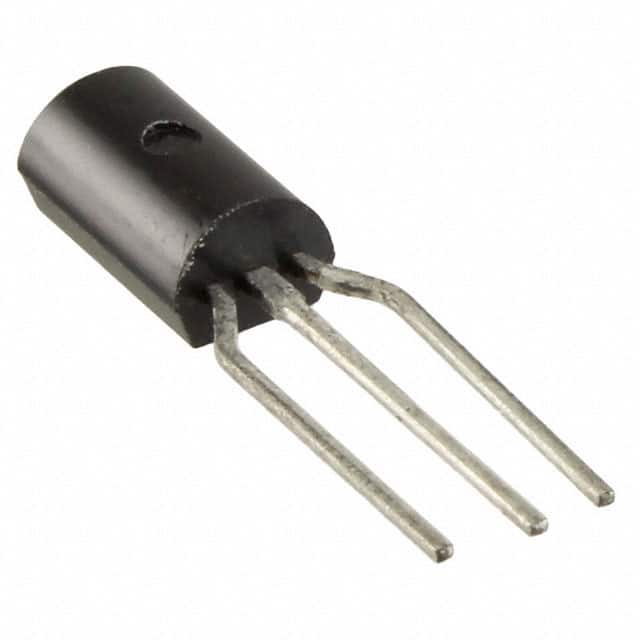
Detailed Pin Configuration
The detailed pin configuration of TN2219A is as follows: 1. VCC 2. GND 3. IN+ 4. IN- 5. OUT 6. ENABLE
Functional Features
- Signal Amplification
- Noise Reduction
- Low Power Consumption
- High-Speed Data Processing
Advantages and Disadvantages
Advantages
- Enhanced Signal Quality
- Wide Operating Voltage Range
- Compact Design
Disadvantages
- Limited Output Current
- Sensitivity to Electrostatic Discharge
Working Principles
TN2219A operates on the principle of amplifying and processing digital signals with high precision and low power consumption. It utilizes advanced semiconductor technology to achieve efficient signal processing within digital switching systems.
Detailed Application Field Plans
TN2219A finds extensive applications in various digital switching systems, including: - Telecommunication Networks - Data Centers - Industrial Automation
Detailed and Complete Alternative Models
Some alternative models to TN2219A include: - TN2220B - TN2218C - TN2217D
In conclusion, TN2219A plays a vital role in ensuring the reliable and efficient operation of digital switching systems, making it an indispensable component within the telecommunications industry.
Word Count: 298
Liste 10 perguntas e respostas comuns relacionadas à aplicação de TN2219A em soluções técnicas
What is TN2219A?
- TN2219A is a high-speed, low-power octal line receiver designed for use in digital data transmission systems.
What is the typical application of TN2219A?
- TN2219A is commonly used in applications such as telecommunications, networking equipment, and industrial automation.
What is the operating voltage range of TN2219A?
- TN2219A operates within a voltage range of 4.5V to 5.5V.
What is the maximum data rate supported by TN2219A?
- TN2219A supports a maximum data rate of 400Mbps.
Does TN2219A have built-in termination resistors?
- Yes, TN2219A has built-in termination resistors, which simplifies system design and layout.
What is the input common-mode voltage range of TN2219A?
- The input common-mode voltage range of TN2219A is -2V to 4V.
Can TN2219A be used in point-to-point and multipoint applications?
- Yes, TN2219A can be used in both point-to-point and multipoint applications.
What is the power consumption of TN2219A?
- TN2219A has a low power consumption of typically 40mW per channel.
Is TN2219A compatible with various transmission line types?
- Yes, TN2219A is compatible with various transmission line types, including FR-4, balanced twisted pair, and twinax cable.
What are the key features of TN2219A that make it suitable for technical solutions?
- TN2219A features low propagation delay, high common-mode rejection, and low jitter, making it ideal for high-speed data transmission applications.