

Veja as especificações para detalhes do produto.
NLAS4599DTT1
Product Overview
Category: Integrated Circuit (IC)
Use: The NLAS4599DTT1 is a versatile analog switch designed for use in various electronic applications. It provides a high-performance solution for signal routing and switching.
Characteristics: - Low ON-resistance - Wide voltage range - High bandwidth - Low power consumption
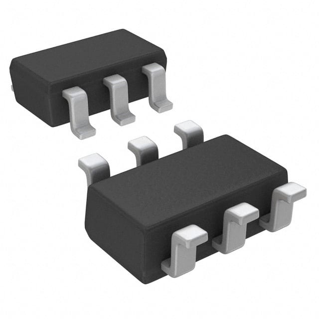
Package: The NLAS4599DTT1 is available in a small form factor package, such as a Thin Shrink Small Outline Package (TSSOP) or a Micro Leadframe Package (MLP). The package ensures easy integration into different circuit designs.
Essence: The essence of the NLAS4599DTT1 lies in its ability to efficiently control the flow of analog signals within a circuit, enabling seamless switching and routing capabilities.
Packaging/Quantity: The NLAS4599DTT1 is typically sold in reels or tubes, with quantities varying depending on the supplier. Common packaging options include 2500 or 3000 units per reel/tube.
Specifications
- Supply Voltage Range: 2.7V to 5.5V
- ON-Resistance (RON): 4Ω (typical)
- Bandwidth: Up to 200MHz
- Leakage Current (ILEAK): 1nA (maximum)
- Control Input Voltage Range: 0V to VCC
- Operating Temperature Range: -40°C to +85°C
Detailed Pin Configuration
The NLAS4599DTT1 features a standard pin configuration with the following pins:
- IN1: Input 1
- IN2: Input 2
- OUT: Output
- VCC: Power Supply
- GND: Ground
Functional Features
- Bidirectional signal switching
- Low power consumption
- High-speed operation
- Break-before-make switching action
- ESD protection on all pins
Advantages and Disadvantages
Advantages: - Low ON-resistance ensures minimal signal attenuation - Wide voltage range allows compatibility with various systems - High bandwidth enables transmission of high-frequency signals - Low power consumption prolongs battery life in portable devices - ESD protection safeguards against electrostatic discharge damage
Disadvantages: - Limited number of channels (only one input/output pair) - Not suitable for high-power applications
Working Principles
The NLAS4599DTT1 operates based on the principle of a metal-oxide-semiconductor field-effect transistor (MOSFET). It utilizes a control voltage to open or close the switch, allowing or blocking the flow of analog signals between the input and output pins.
Detailed Application Field Plans
The NLAS4599DTT1 finds application in various fields, including but not limited to: - Audio and video signal routing - Communication systems - Test and measurement equipment - Industrial automation - Medical devices
Detailed and Complete Alternative Models
- NLAS4599DFT2G
- NLAS4599MNR2G
- NLAS4599MUTAG
- NLAS4599MUTBG
- NLAS4599MUTCG
These alternative models offer similar functionality and performance characteristics as the NLAS4599DTT1, providing flexibility in choosing the most suitable option for specific design requirements.
Note: The above information provides a comprehensive overview of the NLAS4599DTT1. For further technical details and specifications, please refer to the product datasheet provided by the manufacturer.
Liste 10 perguntas e respostas comuns relacionadas à aplicação de NLAS4599DTT1 em soluções técnicas
Sure! Here are 10 common questions and answers related to the application of NLAS4599DTT1 in technical solutions:
1. What is NLAS4599DTT1? NLAS4599DTT1 is a specific type of integrated circuit (IC) that serves as a dual, single-pole, double-throw (DPDT) analog switch.
2. What are the typical applications of NLAS4599DTT1? NLAS4599DTT1 is commonly used in various technical solutions such as audio and video signal routing, data switching, communication systems, and test equipment.
3. What is the voltage range supported by NLAS4599DTT1? NLAS4599DTT1 supports a wide voltage range, typically from -5V to +5V.
4. What is the maximum current handling capability of NLAS4599DTT1? NLAS4599DTT1 can handle currents up to 100mA per channel.
5. Can NLAS4599DTT1 be used with both digital and analog signals? Yes, NLAS4599DTT1 is designed to work with both digital and analog signals, making it versatile for various applications.
6. Does NLAS4599DTT1 require external power supply? No, NLAS4599DTT1 does not require an external power supply as it operates on the voltage supplied by the system.
7. Is NLAS4599DTT1 compatible with different logic families? Yes, NLAS4599DTT1 is compatible with a wide range of logic families, including CMOS, TTL, and LVCMOS.
8. Can NLAS4599DTT1 handle high-frequency signals? Yes, NLAS4599DTT1 has a high bandwidth capability, typically supporting frequencies up to several hundred megahertz (MHz).
9. What is the package type of NLAS4599DTT1? NLAS4599DTT1 is available in various package types, including small-outline integrated circuit (SOIC) and thin shrink small-outline package (TSSOP).
10. Are there any recommended layout considerations for using NLAS4599DTT1? Yes, it is recommended to follow the manufacturer's guidelines for PCB layout, such as proper grounding techniques, minimizing trace lengths, and avoiding noise sources to ensure optimal performance of NLAS4599DTT1.
Please note that the specific details may vary depending on the manufacturer and datasheet specifications of NLAS4599DTT1.