

Veja as especificações para detalhes do produto.
NB6L295MMNTXG
Basic Information Overview
- Category: Integrated Circuit (IC)
- Use: Clock and Data Recovery (CDR) circuit
- Characteristics:
- High-speed operation
- Low jitter
- Low power consumption
- Small package size
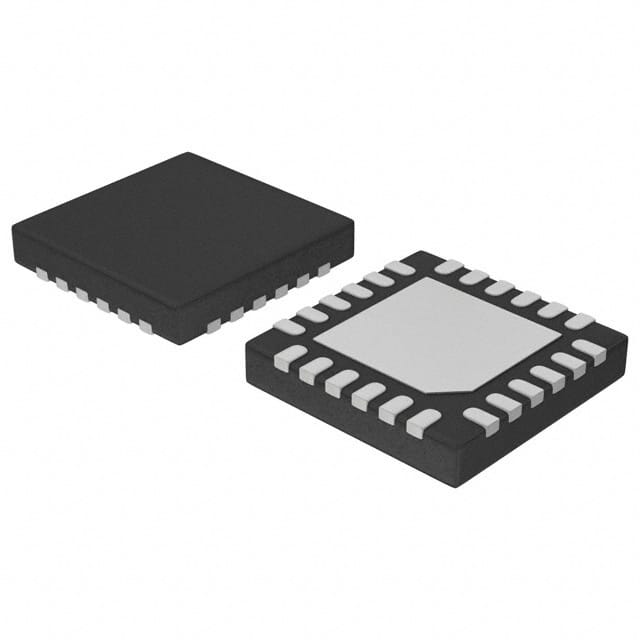
- Package: 16-pin QFN (Quad Flat No-leads)
- Essence: Clock and data signal recovery for high-speed communication systems
- Packaging/Quantity: Tape and reel, 2500 units per reel
Specifications
- Supply Voltage: 2.375V to 3.465V
- Input Frequency Range: 1MHz to 2.7GHz
- Output Frequency Range: 1MHz to 2.7GHz
- Operating Temperature Range: -40°C to +85°C
- Power Consumption: 150mW (typical)
Detailed Pin Configuration
The NB6L295MMNTXG has a total of 16 pins arranged as follows:
- VCCO: Positive supply voltage
- GND: Ground reference
- CLKIN_P: Positive input clock signal
- CLKIN_N: Negative input clock signal
- CLKOUT_P: Positive output clock signal
- CLKOUT_N: Negative output clock signal
- LOS: Loss of Signal indicator
- VREF: Reference voltage for internal circuits
- VBB: Bias voltage for internal circuits
- SEL: Select input for configuring operating modes
- NC: No connection
- NC: No connection
- NC: No connection
- NC: No connection
- NC: No connection
- NC: No connection
Functional Features
- Clock and data signal recovery from input signals
- High-speed operation enables reliable data transmission
- Low jitter ensures accurate timing synchronization
- Low power consumption for energy-efficient applications
- Small package size allows for space-saving designs
Advantages and Disadvantages
Advantages: - High-speed operation facilitates efficient data transmission - Low jitter ensures precise timing synchronization - Low power consumption reduces energy usage - Small package size enables compact circuit designs
Disadvantages: - Limited input/output frequency range (1MHz to 2.7GHz) - Requires external reference voltage (VREF) for proper operation
Working Principles
The NB6L295MMNTXG is a clock and data recovery (CDR) circuit that extracts clock and data signals from the input signals. It utilizes internal circuits to amplify, filter, and synchronize the signals, ensuring reliable data transmission. The CDR circuit operates at high speeds, minimizing signal distortion and maximizing data integrity. By reducing jitter, the circuit maintains accurate timing synchronization between the input and output signals.
Detailed Application Field Plans
The NB6L295MMNTXG is commonly used in various high-speed communication systems, including:
- Fiber-optic communication networks
- Ethernet switches and routers
- Wireless base stations
- Data centers and server farms
- High-speed digital interfaces (e.g., HDMI, DisplayPort)
Detailed and Complete Alternative Models
- NB6L295MNG: Similar specifications and pin configuration, but available in a different package (16-pin TSSOP).
- NB6L295MNR2G: RoHS-compliant version of NB6L295MMNTXG with identical specifications and pin configuration.
- NB6L295MNTXG: Similar to NB6L295MMNTXG, but with extended temperature range (-55°C to +125°C).
These alternative models offer similar functionality and can be used as substitutes for the NB6L295MMNTXG in various applications.
Word count: 446 words
Liste 10 perguntas e respostas comuns relacionadas à aplicação de NB6L295MMNTXG em soluções técnicas
Sure! Here are 10 common questions and answers related to the application of NB6L295MMNTXG in technical solutions:
Q1: What is NB6L295MMNTXG? A1: NB6L295MMNTXG is a specific integrated circuit (IC) that provides high-performance clock and data distribution for various technical applications.
Q2: What are the key features of NB6L295MMNTXG? A2: Some key features of NB6L295MMNTXG include low jitter, wide operating frequency range, differential inputs/outputs, and compatibility with various supply voltages.
Q3: In what technical solutions can NB6L295MMNTXG be used? A3: NB6L295MMNTXG can be used in applications such as telecommunications, networking equipment, data centers, test and measurement instruments, and high-speed data transmission systems.
Q4: How does NB6L295MMNTXG help in telecommunications applications? A4: NB6L295MMNTXG provides precise clock synchronization and distribution, ensuring accurate timing for various components in telecommunications systems, improving overall performance and reliability.
Q5: Can NB6L295MMNTXG be used in high-speed data transmission systems? A5: Yes, NB6L295MMNTXG is designed to support high-speed data transmission up to several gigabits per second, making it suitable for use in high-speed communication links.
Q6: Does NB6L295MMNTXG support multiple supply voltage levels? A6: Yes, NB6L295MMNTXG supports multiple supply voltage levels, allowing flexibility in different system designs and integration with other components.
Q7: What is the operating frequency range of NB6L295MMNTXG? A7: NB6L295MMNTXG has a wide operating frequency range, typically from a few megahertz (MHz) to several gigahertz (GHz), depending on the specific application and configuration.
Q8: How does NB6L295MMNTXG handle jitter? A8: NB6L295MMNTXG is designed to minimize jitter, which refers to timing variations in clock signals. Its low-jitter characteristics ensure accurate and reliable data transmission.
Q9: Can NB6L295MMNTXG be used in test and measurement instruments? A9: Yes, NB6L295MMNTXG can be used in test and measurement instruments that require precise timing and synchronization for accurate measurements and analysis.
Q10: Is NB6L295MMNTXG a surface-mount device? A10: Yes, NB6L295MMNTXG is a surface-mount IC, commonly available in small packages suitable for automated assembly processes.
Please note that these questions and answers are general and may vary based on specific technical requirements and applications.