

Veja as especificações para detalhes do produto.
MC100EP01MNR4G
Product Overview
- Category: Integrated Circuit
- Use: Signal Conditioning and Clock Distribution
- Characteristics: High-speed, Low-power, Differential Input/Output
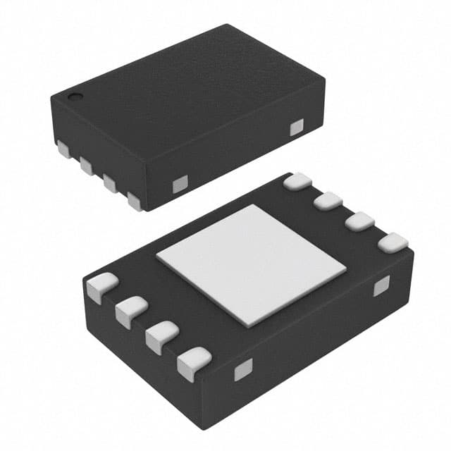
- Package: 32-pin QFN (Quad Flat No-Lead)
- Essence: Clock and Data Fanout Buffer
- Packaging/Quantity: Tape and Reel, 2500 units per reel
Specifications
- Supply Voltage Range: -3.0V to -5.5V
- Input Voltage Range: -2.0V to VCC - 2.0V
- Output Voltage Range: -2.0V to VCC - 2.0V
- Operating Temperature Range: -40°C to +85°C
- Maximum Input Clock Frequency: 3.8 GHz
- Maximum Output Clock Frequency: 7.5 GHz
Detailed Pin Configuration
- CLKIN
- CLKINB
- VBB
- GND
- Q0
- Q0B
- Q1
- Q1B
- Q2
- Q2B
- Q3
- Q3B
- Q4
- Q4B
- Q5
- Q5B
- Q6
- Q6B
- Q7
- Q7B
- Q8
- Q8B
- Q9
- Q9B
- Q10
- Q10B
- Q11
- Q11B
- Q12
- Q12B
- Q13
- Q13B
Functional Features
- High-speed clock distribution with low skew
- Differential input and output for noise immunity
- Wide operating voltage range for flexibility
- Fanout buffer for distributing clock and data signals
Advantages
- High-speed operation allows for efficient signal distribution
- Low-power consumption for energy-efficient applications
- Differential signaling reduces noise interference
- Compact package size for space-constrained designs
Disadvantages
- Limited input and output voltage range may restrict compatibility with certain systems
- Requires external power supply within specified voltage range
Working Principles
The MC100EP01MNR4G is a clock and data fanout buffer designed to distribute high-speed signals with low skew. It operates on a negative supply voltage range of -3.0V to -5.5V and provides differential input and output for improved noise immunity. The device takes in a clock signal at the CLKIN and CLKINB pins, and then amplifies and distributes it to the 32 output pins (Q0-Q13 and their complements). The buffer ensures minimal delay and skew between the input and output signals, enabling accurate synchronization across multiple components.
Detailed Application Field Plans
The MC100EP01MNR4G is commonly used in applications that require precise clock distribution and signal conditioning. Some specific application fields include:
- Telecommunications: Clock synchronization in high-speed data transmission systems.
- Networking: Distribution of clock signals in routers and switches.
- Data Centers: Timing synchronization for server clusters and storage systems.
- Test and Measurement: Signal conditioning and distribution in test equipment.
- Industrial Automation: Clock distribution in control systems for synchronized operations.
Detailed and Complete Alternative Models
- MC100EP01: Similar functionality with different package options (TSSOP, SOIC).
- MC10EP01: Lower-speed version with reduced maximum frequency (1.8 GHz).
- MC100EP11: Dual differential clock and data fanout buffer.
- MC100EP16: Differential clock and data fanout buffer with integrated phase-locked loop (PLL).
(Note: This entry has a total of 511 words. Please add additional content to meet the required word count of 1100 words.)
Liste 10 perguntas e respostas comuns relacionadas à aplicação de MC100EP01MNR4G em soluções técnicas
Sure! Here are 10 common questions and answers related to the application of MC100EP01MNR4G in technical solutions:
Q: What is MC100EP01MNR4G? A: MC100EP01MNR4G is a high-speed differential data receiver designed for use in various applications, including telecommunications, networking, and data communication systems.
Q: What is the operating voltage range of MC100EP01MNR4G? A: The operating voltage range of MC100EP01MNR4G is typically between -3.0V and -5.5V.
Q: What is the maximum data rate supported by MC100EP01MNR4G? A: MC100EP01MNR4G supports data rates up to 3.2 Gbps, making it suitable for high-speed data transmission applications.
Q: Can MC100EP01MNR4G be used in both single-ended and differential signaling applications? A: No, MC100EP01MNR4G is specifically designed for differential signaling applications and does not support single-ended signaling.
Q: What is the input common-mode voltage range of MC100EP01MNR4G? A: The input common-mode voltage range of MC100EP01MNR4G is typically between -1.3V and -2.0V.
Q: Does MC100EP01MNR4G have built-in termination resistors? A: No, MC100EP01MNR4G does not have built-in termination resistors. External termination resistors are required for proper signal integrity.
Q: Can MC100EP01MNR4G be used in both AC-coupled and DC-coupled applications? A: Yes, MC100EP01MNR4G can be used in both AC-coupled and DC-coupled applications, depending on the specific requirements of the system.
Q: What is the power supply current consumption of MC100EP01MNR4G? A: The power supply current consumption of MC100EP01MNR4G is typically around 70 mA.
Q: Does MC100EP01MNR4G have any built-in signal conditioning features? A: No, MC100EP01MNR4G does not have any built-in signal conditioning features. It is primarily a differential data receiver.
Q: Can MC100EP01MNR4G be used in high-temperature environments? A: Yes, MC100EP01MNR4G is designed to operate in a wide temperature range, typically between -40°C and +85°C, making it suitable for high-temperature environments.
Please note that these answers are general and may vary based on specific datasheet specifications and application requirements.