

Veja as especificações para detalhes do produto.
M74VHC1G125DTT1G
Product Overview
- Category: Integrated Circuit (IC)
- Use: Logic Level Shifter
- Characteristics: High-speed, low-power consumption
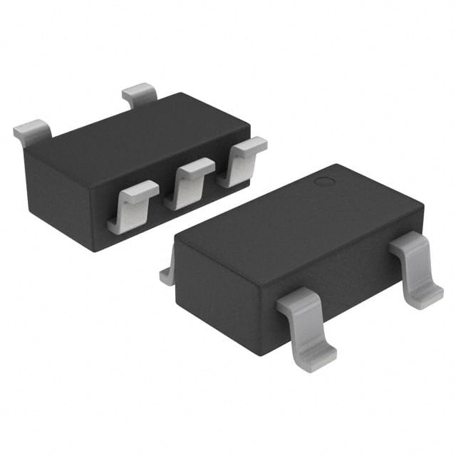
- Package: SOT-23-5
- Essence: Single gate non-inverting buffer
- Packaging/Quantity: Tape and Reel, 3000 pieces per reel
Specifications
- Supply Voltage: 2.0V to 5.5V
- Input Voltage: 0V to VCC
- Output Voltage: 0V to VCC
- Operating Temperature: -40°C to +125°C
- Propagation Delay: 3.5ns (typical)
- Output Current: ±8mA
Detailed Pin Configuration
The M74VHC1G125DTT1G has a total of 5 pins:
- GND (Ground): Connected to the ground reference of the circuit.
- A (Input): Input pin for the logic signal to be shifted.
- Y (Output): Output pin for the shifted logic signal.
- OE (Output Enable): Control pin to enable or disable the output.
- VCC (Power Supply): Connected to the positive supply voltage.
Functional Features
- Provides level shifting capability between different logic voltage domains.
- Non-inverting buffer ensures the same logic polarity at the output as the input.
- High-speed operation allows for efficient data transmission.
- Low-power consumption makes it suitable for battery-powered devices.
- Output enable pin allows for easy control of the output state.
Advantages and Disadvantages
Advantages: - Compact SOT-23-5 package saves board space. - Wide operating voltage range enables compatibility with various systems. - Fast propagation delay ensures quick signal transmission. - Low power consumption extends battery life in portable applications.
Disadvantages: - Limited output current may not be suitable for driving heavy loads. - Single gate configuration restricts the number of logic functions it can perform.
Working Principles
The M74VHC1G125DTT1G is a single gate non-inverting buffer. It operates by receiving a logic signal at the input pin (A) and amplifying it to the output pin (Y). The output state can be controlled using the output enable pin (OE). When OE is high, the output follows the input signal. When OE is low, the output is disabled and remains in a high-impedance state.
Detailed Application Field Plans
The M74VHC1G125DTT1G is commonly used in various digital systems where level shifting is required. Some application fields include:
- Microcontrollers and microprocessors
- Communication systems
- Data acquisition systems
- Industrial automation
- Consumer electronics
Detailed and Complete Alternative Models
- SN74LVC1G125DBVR - Single gate non-inverting buffer with Schmitt-trigger inputs.
- NC7SZ125P5X - Single gate non-inverting buffer with 5-pin SC-70 package.
- TC7SZ125FU - Single gate non-inverting buffer with ultra-small VSSOP-5 package.
These alternative models offer similar functionality and can be considered as substitutes for the M74VHC1G125DTT1G in different applications.
Word count: 420 words
Liste 10 perguntas e respostas comuns relacionadas à aplicação de M74VHC1G125DTT1G em soluções técnicas
Sure! Here are 10 common questions and answers related to the application of M74VHC1G125DTT1G in technical solutions:
Q1: What is the M74VHC1G125DTT1G? A1: The M74VHC1G125DTT1G is a single bus buffer gate with 3-state output, designed for use in various digital applications.
Q2: What is the operating voltage range of M74VHC1G125DTT1G? A2: The operating voltage range of M74VHC1G125DTT1G is typically between 2.0V and 5.5V.
Q3: What is the maximum output current of M74VHC1G125DTT1G? A3: The maximum output current of M74VHC1G125DTT1G is typically around 8mA.
Q4: Can I use M74VHC1G125DTT1G for level shifting purposes? A4: Yes, M74VHC1G125DTT1G can be used for level shifting as it supports both TTL and CMOS logic levels.
Q5: What is the propagation delay of M74VHC1G125DTT1G? A5: The propagation delay of M74VHC1G125DTT1G is typically around 4.5ns.
Q6: Is M74VHC1G125DTT1G suitable for high-speed applications? A6: Yes, M74VHC1G125DTT1G is suitable for high-speed applications due to its fast switching characteristics.
Q7: Can I connect multiple M74VHC1G125DTT1G devices in parallel? A7: Yes, you can connect multiple M74VHC1G125DTT1G devices in parallel to increase the output current capability.
Q8: Does M74VHC1G125DTT1G have built-in protection features? A8: Yes, M74VHC1G125DTT1G has built-in ESD protection and can withstand electrostatic discharges up to 2kV.
Q9: What is the package type of M74VHC1G125DTT1G? A9: M74VHC1G125DTT1G is available in a small SOT-23 package.
Q10: Can I use M74VHC1G125DTT1G in battery-powered applications? A10: Yes, M74VHC1G125DTT1G can be used in battery-powered applications as it operates within a wide voltage range and has low power consumption.
Please note that the answers provided here are general and may vary depending on specific datasheet specifications and application requirements.