

Veja as especificações para detalhes do produto.
Encyclopedia Entry: 74LVT374MTCX
Product Overview
Category
The 74LVT374MTCX belongs to the category of integrated circuits (ICs) and specifically falls under the family of flip-flops.
Use
This IC is commonly used in digital electronics for storing and transferring binary data. It serves as a latch or register, allowing for the temporary storage and manipulation of information within a circuit.
Characteristics
- Low-voltage operation: The 74LVT374MTCX operates at low voltage levels, typically between 2.7V and 3.6V.
- High-speed performance: It offers fast data transfer rates, making it suitable for applications requiring quick data processing.
- Tri-state outputs: The IC features tri-state outputs, enabling efficient bus sharing and reducing signal interference.
- D-type flip-flop: It consists of eight D-type flip-flops, each capable of storing one bit of data.
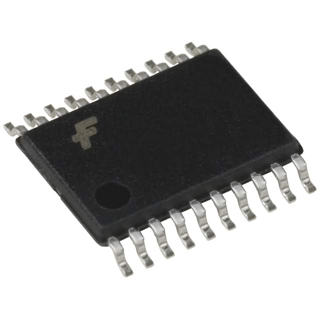
Package and Quantity
The 74LVT374MTCX is available in a small outline integrated circuit (SOIC) package. It comes in a tape and reel packaging, with a standard quantity of 250 units per reel.
Specifications
- Supply Voltage Range: 2.7V to 3.6V
- Input Voltage Range: 0V to Vcc
- Output Voltage Range: 0V to Vcc
- Operating Temperature Range: -40°C to +85°C
- Maximum Clock Frequency: 200 MHz
- Propagation Delay: 4 ns (typical)
Pin Configuration
The 74LVT374MTCX has a total of 20 pins, which are assigned specific functions as follows:
- OE (Output Enable)
- Q0 (Flip-Flop Output 0)
- D0 (Data Input 0)
- D1 (Data Input 1)
- Q1 (Flip-Flop Output 1)
- D2 (Data Input 2)
- D3 (Data Input 3)
- Q2 (Flip-Flop Output 2)
- GND (Ground)
- Q3 (Flip-Flop Output 3)
- D4 (Data Input 4)
- D5 (Data Input 5)
- Q4 (Flip-Flop Output 4)
- D6 (Data Input 6)
- D7 (Data Input 7)
- Q5 (Flip-Flop Output 5)
- Vcc (Power Supply)
- Q6 (Flip-Flop Output 6)
- Q7 (Flip-Flop Output 7)
- CP (Clock Pulse)
Functional Features
The 74LVT374MTCX offers the following functional features:
- Edge-triggered operation: The flip-flops within the IC are triggered by the rising edge of the clock pulse, allowing for synchronized data storage and transfer.
- Tri-state outputs: The tri-state outputs enable multiple devices to share a common bus, reducing the number of required interconnections.
- High-speed operation: With a maximum clock frequency of 200 MHz, this IC can handle rapid data processing tasks efficiently.
Advantages and Disadvantages
Advantages
- Low-voltage operation makes it suitable for battery-powered applications.
- Tri-state outputs facilitate efficient bus sharing and reduce signal interference.
- High-speed performance enables quick data processing.
Disadvantages
- Limited voltage range may restrict compatibility with certain systems.
- Sensitivity to electrostatic discharge (ESD) requires proper handling during installation and usage.
Working Principles
The 74LVT374MTCX operates based on the principles of D-type flip-flops. When a clock pulse is received, the data present at the input pins (D0-D7) is latched and stored in the corresponding flip-flops. The stored data can then be accessed from the output pins (Q0-Q7). The tri-state outputs allow for enabling or disabling the output signals, providing control over the data flow.
Application Field Plans
The 74LVT374MTCX finds applications in various digital systems, including but not limited to:
- Microprocessors and microcontrollers
- Data storage devices
- Communication systems
- Digital signal processing
- Industrial automation
Alternative Models
For those seeking alternative options, the following ICs can be considered as substitutes for the 74LVT374MTCX:
- SN74LVC374A: This IC offers similar functionality and characteristics, with compatibility across a wider voltage range.
- CD74HCT374: A high-speed CMOS logic IC that provides comparable features and performance.
- MC74LVX374: Another low-voltage octal D-type flip-flop IC suitable for similar applications.
These alternatives offer similar functionalities and
Liste 10 perguntas e respostas comuns relacionadas à aplicação de 74LVT374MTCX em soluções técnicas
Sure! Here are 10 common questions and answers related to the application of 74LVT374MTCX in technical solutions:
Q: What is the function of the 74LVT374MTCX? A: The 74LVT374MTCX is an octal D-type flip-flop with 3-state outputs, used for storing and transferring data in digital circuits.
Q: What is the operating voltage range of the 74LVT374MTCX? A: The 74LVT374MTCX operates within a voltage range of 2.7V to 3.6V.
Q: How many flip-flops are there in the 74LVT374MTCX? A: The 74LVT374MTCX contains 8 flip-flops, making it an octal (8-bit) device.
Q: What is the maximum clock frequency supported by the 74LVT374MTCX? A: The 74LVT374MTCX can operate at a maximum clock frequency of 200 MHz.
Q: Can I use the 74LVT374MTCX in both synchronous and asynchronous applications? A: Yes, the 74LVT374MTCX can be used in both synchronous and asynchronous applications.
Q: What is the output drive capability of the 74LVT374MTCX? A: The 74LVT374MTCX has a typical output drive capability of ±24mA.
Q: Does the 74LVT374MTCX support 3-state outputs? A: Yes, the 74LVT374MTCX supports 3-state outputs, allowing multiple devices to share a common bus.
Q: Can I cascade multiple 74LVT374MTCX devices together? A: Yes, you can cascade multiple 74LVT374MTCX devices to increase the number of flip-flops in your circuit.
Q: What is the power supply voltage tolerance of the 74LVT374MTCX? A: The 74LVT374MTCX has a power supply voltage tolerance of ±0.3V.
Q: Is the 74LVT374MTCX available in different package options? A: Yes, the 74LVT374MTCX is available in various package options, including TSSOP and SOIC.
Please note that these answers are general and may vary depending on the specific datasheet and manufacturer's specifications for the 74LVT374MTCX.