

Veja as especificações para detalhes do produto.
Encyclopedia Entry: 74ACT16374SSC
Product Information Overview
- Category: Integrated Circuit (IC)
- Use: Digital Logic
- Characteristics: High-speed, low-power, 16-bit D-type flip-flop with 3-state outputs
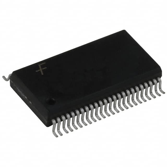
- Package: SSOP (Shrink Small Outline Package)
- Essence: Flip-flop with 3-state outputs
- Packaging/Quantity: Available in reels or tubes, quantity varies based on manufacturer
Specifications
- Number of Bits: 16
- Logic Family: ACT (Advanced CMOS Technology)
- Supply Voltage: 2.0V to 6.0V
- Operating Temperature Range: -40°C to +85°C
- Output Type: 3-state
- Propagation Delay: 4.5 ns (typical)
- Input/Output Compatibility: TTL (Transistor-Transistor Logic) and CMOS (Complementary Metal-Oxide-Semiconductor)
Detailed Pin Configuration
The 74ACT16374SSC IC has a total of 48 pins, which are divided into four groups:
Group A (Pins 1-12)
- Pin 1: Output Enable (OE)
- Pin 2: Data Input (D0)
- Pin 3: Data Input (D1)
- Pin 4: Data Input (D2)
- Pin 5: Data Input (D3)
- Pin 6: Data Input (D4)
- Pin 7: Data Input (D5)
- Pin 8: Data Input (D6)
- Pin 9: Data Input (D7)
- Pin 10: Data Input (D8)
- Pin 11: Data Input (D9)
- Pin 12: Data Input (D10)
Group B (Pins 13-24)
- Pin 13: Data Input (D11)
- Pin 14: Data Input (D12)
- Pin 15: Data Input (D13)
- Pin 16: Data Input (D14)
- Pin 17: Data Input (D15)
- Pin 18: Clock Input (CP0)
- Pin 19: Clock Input (CP1)
- Pin 20: Clock Enable (CE)
- Pin 21: Master Reset (MR)
- Pin 22: Output Enable (OE)
- Pin 23: 3-state Output (Q0)
- Pin 24: 3-state Output (Q1)
Group C (Pins 25-36)
- Pin 25: 3-state Output (Q2)
- Pin 26: 3-state Output (Q3)
- Pin 27: 3-state Output (Q4)
- Pin 28: 3-state Output (Q5)
- Pin 29: 3-state Output (Q6)
- Pin 30: 3-state Output (Q7)
- Pin 31: 3-state Output (Q8)
- Pin 32: 3-state Output (Q9)
- Pin 33: 3-state Output (Q10)
- Pin 34: 3-state Output (Q11)
- Pin 35: 3-state Output (Q12)
- Pin 36: 3-state Output (Q13)
Group D (Pins 37-48)
- Pin 37: 3-state Output (Q14)
- Pin 38: 3-state Output (Q15)
- Pin 39: Ground (GND)
- Pin 40: Supply Voltage (VCC)
- Pins 41-48: No Connection (NC)
Functional Features
- 16-bit D-type flip-flop with 3-state outputs
- High-speed operation with low power consumption
- Compatible with both TTL and CMOS logic levels
- Output enable and clock enable inputs for flexible control
- Master reset input for synchronous reset of all flip-flops
Advantages and Disadvantages
Advantages
- High-speed performance allows for efficient data processing
- Low-power consumption helps in reducing energy usage
- Compatibility with both TTL and CMOS logic levels provides versatility in system integration
- Flexible control through output enable, clock enable, and master reset inputs
Disadvantages
- Limited number of flip-flops (16 bits) may not be suitable for applications requiring larger data storage
- Sensitive to voltage fluctuations, requiring stable power supply for reliable operation
Working Principles
The 74ACT16374SSC is a 16-bit D-type flip-flop with 3-state outputs. It operates based on the principles of digital logic, where the flip-flops store and manipulate binary data. The input data is latched into the flip-flops on the rising edge of the clock signal
Liste 10 perguntas e respostas comuns relacionadas à aplicação de 74ACT16374SSC em soluções técnicas
Sure! Here are 10 common questions and answers related to the application of 74ACT16374SSC in technical solutions:
Q: What is the 74ACT16374SSC? A: The 74ACT16374SSC is a 16-bit D-type flip-flop with 3-state outputs, commonly used in digital circuits.
Q: What are the key features of the 74ACT16374SSC? A: Some key features include high-speed operation, 3-state outputs for bus-oriented applications, and compatibility with TTL input levels.
Q: How can I use the 74ACT16374SSC in my circuit design? A: You can use it as a storage element or for data transfer between different parts of your circuit.
Q: Can I cascade multiple 74ACT16374SSC devices together? A: Yes, you can cascade multiple devices to increase the number of bits in your circuit.
Q: What is the maximum clock frequency supported by the 74ACT16374SSC? A: The maximum clock frequency typically depends on the specific datasheet specifications, but it is usually in the range of several hundred megahertz.
Q: How do I connect the inputs and outputs of the 74ACT16374SSC? A: The inputs are connected to the data source, clock signal, and control signals, while the outputs can be connected to other parts of the circuit or external devices.
Q: Can I use the 74ACT16374SSC in both synchronous and asynchronous applications? A: Yes, the 74ACT16374SSC can be used in both synchronous and asynchronous applications, depending on how you configure the clock and control signals.
Q: What is the power supply voltage range for the 74ACT16374SSC? A: The typical power supply voltage range is between 4.5V and 5.5V, but it's important to refer to the specific datasheet for accurate information.
Q: Are there any special considerations for PCB layout when using the 74ACT16374SSC? A: Yes, it's recommended to follow proper PCB layout guidelines to minimize noise, ensure signal integrity, and optimize performance.
Q: Where can I find more detailed information about the 74ACT16374SSC? A: You can refer to the manufacturer's datasheet, application notes, or technical documentation for more detailed information on the device's specifications, timing diagrams, and recommended usage guidelines.
Please note that the answers provided here are general and may vary depending on the specific implementation and requirements of your technical solution.