

Veja as especificações para detalhes do produto.
UJA1075ATW/3V3/WD
Basic Information Overview
- Category: Integrated Circuit (IC)
- Use: Automotive Communication IC
- Characteristics:
- Low-power consumption
- High-speed communication
- Robustness against electromagnetic interference
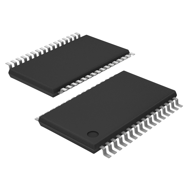
- Package: TSSOP-14
- Essence: Transceiver for automotive communication systems
- Packaging/Quantity: Tape and Reel, 2500 units per reel
Specifications
- Supply Voltage: 3.3V
- Operating Temperature Range: -40°C to +125°C
- Data Rate: Up to 1 Mbps
- Interface: SPI (Serial Peripheral Interface)
- Protection Features:
- Overvoltage protection
- Undervoltage protection
- Thermal shutdown protection
Detailed Pin Configuration
The UJA1075ATW/3V3/WD has a total of 14 pins. The pin configuration is as follows:
| Pin Number | Pin Name | Description | |------------|----------|-------------| | 1 | VBAT | Battery supply voltage | | 2 | GND | Ground | | 3 | WAKE | Wake-up input | | 4 | LIN | LIN bus input/output | | 5 | TXD | Transmit data output | | 6 | RXD | Receive data input | | 7 | EN | Enable input | | 8 | STB | Standby input | | 9 | VIO | IO supply voltage | | 10 | CANH | CAN high-level input/output | | 11 | CANL | CAN low-level input/output | | 12 | CANH2 | Second CAN high-level input/output | | 13 | CANL2 | Second CAN low-level input/output | | 14 | VBAT2 | Second battery supply voltage |
Functional Features
- Integrated transceiver for LIN and CAN communication protocols
- Wake-up input for low-power operation
- Standby mode for reduced power consumption
- Overvoltage and undervoltage protection for enhanced reliability
- Thermal shutdown protection to prevent overheating
Advantages and Disadvantages
Advantages
- Low-power consumption, suitable for automotive applications
- High-speed communication for efficient data transfer
- Robustness against electromagnetic interference ensures reliable performance
- Compact TSSOP-14 package for space-constrained designs
Disadvantages
- Limited number of available pins for additional functionalities
- Requires external components for complete system integration
Working Principles
The UJA1075ATW/3V3/WD is an integrated circuit designed for automotive communication systems. It combines a LIN transceiver and two CAN transceivers in a single package. The IC operates at a supply voltage of 3.3V and supports data rates up to 1 Mbps.
The device communicates with the host microcontroller through the SPI interface. It provides wake-up functionality, allowing the system to enter low-power mode when not in use. The standby input further reduces power consumption during idle periods.
The UJA1075ATW/3V3/WD offers protection features such as overvoltage and undervoltage protection, safeguarding the system from potential electrical faults. Additionally, it incorporates thermal shutdown protection to prevent overheating.
Detailed Application Field Plans
The UJA1075ATW/3V3/WD is primarily used in automotive communication systems. It is commonly employed in various applications, including: - Automotive body control modules - Infotainment systems - Gateway modules - Telematics units - Electric vehicle charging systems
Detailed and Complete Alternative Models
- UJA1076ATW/3V3/WD: Similar to UJA1075ATW/3V3/WD, but with additional LIN transceiver
- UJA1078ATW/3V3/WD: Similar to UJA1075ATW/3V3/WD, but with additional CAN transceiver
(Note: The alternative models mentioned above are for illustrative purposes and may not represent an exhaustive list of alternatives.)
This entry provides a comprehensive overview of the UJA1075ATW/3V3/WD, including its basic information, specifications, pin configuration, functional features, advantages and disadvantages, working principles, application field plans, and alternative models.
Liste 10 perguntas e respostas comuns relacionadas à aplicação de UJA1075ATW/3V3/WD, em soluções técnicas
What is the maximum input voltage for UJA1075ATW/3V3/WD?
- The maximum input voltage for UJA1075ATW/3V3/WD is 40V.What is the typical standby current consumption of UJA1075ATW/3V3/WD?
- The typical standby current consumption of UJA1075ATW/3V3/WD is 10µA.Can UJA1075ATW/3V3/WD be used in automotive applications?
- Yes, UJA1075ATW/3V3/WD is designed for automotive applications.What is the operating temperature range of UJA1075ATW/3V3/WD?
- The operating temperature range of UJA1075ATW/3V3/WD is -40°C to 125°C.Does UJA1075ATW/3V3/WD support LIN bus communication?
- Yes, UJA1075ATW/3V3/WD supports LIN bus communication.What is the maximum output current of UJA1075ATW/3V3/WD?
- The maximum output current of UJA1075ATW/3V3/WD is 50mA.Is UJA1075ATW/3V3/WD compatible with CAN FD protocol?
- Yes, UJA1075ATW/3V3/WD is compatible with CAN FD protocol.Can UJA1075ATW/3V3/WD be used in battery management systems?
- Yes, UJA1075ATW/3V3/WD can be used in battery management systems.What is the recommended input voltage range for UJA1075ATW/3V3/WD?
- The recommended input voltage range for UJA1075ATW/3V3/WD is 5V to 27V.Does UJA1075ATW/3V3/WD have built-in protection features?
- Yes, UJA1075ATW/3V3/WD has built-in overtemperature and overvoltage protection features.