

Veja as especificações para detalhes do produto.
Encyclopedia Entry: 74LVT32374EC/G,518
Product Information Overview
Category: Integrated Circuit (IC)
Use: The 74LVT32374EC/G,518 is a high-speed, low-voltage, 32-bit D-type flip-flop with 3-state outputs. It is designed for use in various digital applications where data storage and signal transmission are required.
Characteristics: This IC operates at a low voltage level, making it suitable for battery-powered devices. It offers high-speed data transfer capabilities and features 3-state outputs, allowing multiple devices to share a common bus without interference. The 74LVT32374EC/G,518 is known for its reliability and compatibility with different logic families.
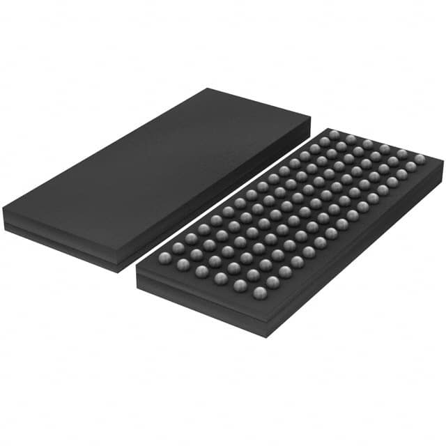
Package: The 74LVT32374EC/G,518 is available in an industry-standard 48-pin TSSOP (Thin Shrink Small Outline Package) package. This package provides excellent thermal performance and ease of handling during assembly.
Essence: The essence of the 74LVT32374EC/G,518 lies in its ability to store and transmit digital data efficiently, while maintaining compatibility with various logic families and operating at a low voltage level.
Packaging/Quantity: The 74LVT32374EC/G,518 is typically sold in reels or tubes containing multiple units. The exact quantity may vary depending on the supplier.
Specifications
- Supply Voltage Range: 2.7V to 3.6V
- High-Speed Operation: 8ns maximum propagation delay
- Output Drive Capability: ±24mA
- Operating Temperature Range: -40°C to +85°C
- Input/Output Compatibility: TTL, LVTTL, LVCMOS
Detailed Pin Configuration
The 74LVT32374EC/G,518 has a total of 48 pins, each serving a specific function. Here is a detailed pin configuration:
- Pin 1: Output Enable (OE)
- Pin 2: Data Input (D0)
- Pin 3: Data Input (D1)
- Pin 4: Data Input (D2)
- Pin 5: Data Input (D3)
- Pin 6: Data Input (D4)
- Pin 7: Data Input (D5)
- Pin 8: Data Input (D6)
- Pin 9: Data Input (D7)
- Pin 10: Data Input (D8)
- Pin 11: Data Input (D9)
- Pin 12: Data Input (D10)
- Pin 13: Data Input (D11)
- Pin 14: Data Input (D12)
- Pin 15: Data Input (D13)
- Pin 16: Data Input (D14)
- Pin 17: Data Input (D15)
- Pin 18: Output (Q0)
- Pin 19: Output (Q1)
- Pin 20: Output (Q2)
- Pin 21: Output (Q3)
- Pin 22: Output (Q4)
- Pin 23: Output (Q5)
- Pin 24: Output (Q6)
- Pin 25: Output (Q7)
- Pin 26: Output (Q8)
- Pin 27: Output (Q9)
- Pin 28: Output (Q10)
- Pin 29: Output (Q11)
- Pin 30: Output (Q12)
- Pin 31: Output (Q13)
- Pin 32: Output (Q14)
- Pin 33: Output (Q15)
- Pin 34: Clock Input (CP)
- Pin 35: Clock Enable (CE)
- Pin 36: Master Reset (MR)
- Pin 37: GND (Ground)
- Pin 38: GND (Ground)
- Pin 39: Data Output Enable (DOE)
- Pin 40: VCC (Positive Power Supply) 41-48. Reserved for future use
Functional Features
The 74LVT32374EC/G,518 offers the following functional features:
- Data Storage: It can store 32 bits of digital data using D-type flip-flops.
- Signal Transmission: The IC allows efficient transmission of stored data to the output pins.
- Output Control: The 3-state outputs enable multiple devices to share a common bus without interference.
- Compatibility: It is compatible with various logic families such as TTL, LVTTL, and LVCMOS.
- High-Speed Operation: With a maximum propagation delay of 8ns, it ensures fast data transfer.
Advantages and Disadvantages
Liste 10 perguntas e respostas comuns relacionadas à aplicação de 74LVT32374EC/G,518 em soluções técnicas
What is the maximum operating voltage for 74LVT32374EC/G,518?
- The maximum operating voltage for 74LVT32374EC/G,518 is 3.6V.What is the typical input high threshold voltage for 74LVT32374EC/G,518?
- The typical input high threshold voltage for 74LVT32374EC/G,518 is 2.3V.What is the output drive capability of 74LVT32374EC/G,518?
- 74LVT32374EC/G,518 has a balanced output drive with 24mA sink and source capability.Can 74LVT32374EC/G,518 be used in automotive applications?
- Yes, 74LVT32374EC/G,518 is suitable for automotive applications.What is the maximum propagation delay of 74LVT32374EC/G,518?
- The maximum propagation delay of 74LVT32374EC/G,518 is 5.5ns.Is 74LVT32374EC/G,518 compatible with both CMOS and TTL input levels?
- Yes, 74LVT32374EC/G,518 is compatible with both CMOS and TTL input levels.What is the operating temperature range for 74LVT32374EC/G,518?
- 74LVT32374EC/G,518 has an operating temperature range of -40°C to 85°C.Can 74LVT32374EC/G,518 be used in battery-powered applications?
- Yes, 74LVT32374EC/G,518 is suitable for battery-powered applications due to its low power consumption.Does 74LVT32374EC/G,518 have built-in ESD protection?
- Yes, 74LVT32374EC/G,518 features built-in ESD protection on all pins.What is the package type for 74LVT32374EC/G,518?
- 74LVT32374EC/G,518 is available in a TSSOP package.