

Veja as especificações para detalhes do produto.
74HC7403D,518
Product Overview
- Category: Integrated Circuit (IC)
- Use: Logic Gate
- Characteristics: High-speed, CMOS technology
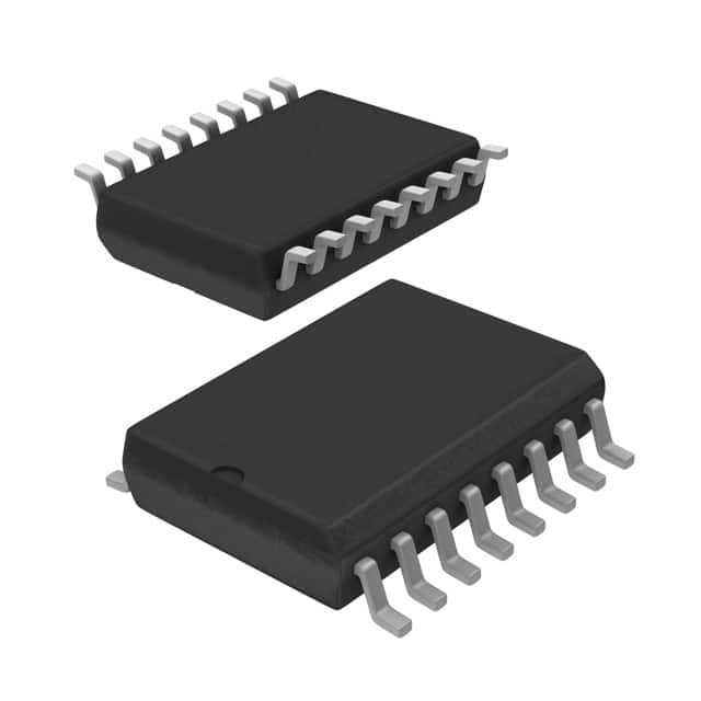
- Package: SOIC (Small Outline Integrated Circuit)
- Essence: Quad 2-input NAND gate
- Packaging/Quantity: Tape and Reel, 2500 units per reel
Specifications
- Supply Voltage: 2V to 6V
- Input Voltage: 0V to VCC
- Output Voltage: 0V to VCC
- Operating Temperature Range: -40°C to +125°C
- Propagation Delay: 10 ns (typical)
- Input Capacitance: 3.5 pF (typical)
- Output Current: ±25 mA
Detailed Pin Configuration
The 74HC7403D,518 has a total of 14 pins arranged as follows:
__    __
   A1 -| 1    14 |- VCC
   A2 -| 2    13 |- B1
   B2 -| 3    12 |- B3
   Y1 -| 4    11 |- A3
   Y2 -| 5    10 |- A4
  GND -| 6     9 |- Y3
  GND -| 7     8 |- Y4
       |_________|
Functional Features
- Quad 2-input NAND gate with Schmitt-trigger inputs
- High-speed operation due to CMOS technology
- Wide operating voltage range
- Low power consumption
- Schmitt-trigger inputs provide hysteresis for improved noise immunity
- Compatible with TTL levels
Advantages and Disadvantages
Advantages: - High-speed operation - Wide operating voltage range - Low power consumption - Improved noise immunity
Disadvantages: - Limited number of inputs (2 per gate) - Not suitable for high-current applications
Working Principles
The 74HC7403D,518 is a quad 2-input NAND gate that utilizes CMOS technology. It operates by taking two input signals and producing an inverted output signal. The Schmitt-trigger inputs provide hysteresis, which helps in reducing the effects of noise and ensuring reliable operation.
Detailed Application Field Plans
The 74HC7403D,518 can be used in various digital logic applications such as:
- Data processing systems
- Communication equipment
- Industrial control systems
- Automotive electronics
- Consumer electronics
Detailed and Complete Alternative Models
Some alternative models to the 74HC7403D,518 include:
- 74LS00: Quad 2-input NAND gate with TTL technology
- CD4011: Quad 2-input NAND gate with CMOS technology
- SN74LVC2G00: Dual 2-input NAND gate with low-voltage CMOS technology
These alternative models offer similar functionality but may have different specifications and package options.
Word count: 275 words
Liste 10 perguntas e respostas comuns relacionadas à aplicação de 74HC7403D,518 em soluções técnicas
Sure! Here are 10 common questions and answers related to the application of 74HC7403D,518 in technical solutions:
Q: What is the 74HC7403D,518? A: The 74HC7403D,518 is a quad 2-input NAND gate IC (integrated circuit) that can be used in various digital logic applications.
Q: What is the operating voltage range for the 74HC7403D,518? A: The operating voltage range for the 74HC7403D,518 is typically between 2V and 6V.
Q: How many gates are there in the 74HC7403D,518? A: The 74HC7403D,518 contains four independent NAND gates.
Q: What is the maximum output current of the 74HC7403D,518? A: The maximum output current per gate of the 74HC7403D,518 is around 4mA.
Q: Can the 74HC7403D,518 be used in both TTL and CMOS logic systems? A: Yes, the 74HC7403D,518 is compatible with both TTL (Transistor-Transistor Logic) and CMOS (Complementary Metal-Oxide-Semiconductor) logic systems.
Q: What is the propagation delay of the 74HC7403D,518? A: The typical propagation delay of the 74HC7403D,518 is around 9 ns.
Q: Can the 74HC7403D,518 be used as an inverter? A: Yes, by connecting one input of the NAND gate to its output, it can function as an inverter.
Q: What is the pin configuration of the 74HC7403D,518? A: The 74HC7403D,518 has a standard 14-pin DIP (Dual Inline Package) configuration.
Q: Can the 74HC7403D,518 be used in high-speed applications? A: Yes, the 74HC7403D,518 is designed for high-speed operation and can be used in various high-frequency applications.
Q: Are there any specific precautions to consider when using the 74HC7403D,518? A: It is important to ensure that the power supply voltage does not exceed the specified limits and to avoid static discharge during handling to prevent damage to the IC.
Please note that the answers provided here are general and may vary depending on the specific datasheet and manufacturer's specifications for the 74HC7403D,518.