

Veja as especificações para detalhes do produto.
74LVC4245ABQ-Q100J
Basic Information Overview
- Category: Integrated Circuit (IC)
- Use: Level Shifter and Bus Transceiver
- Characteristics: Bi-directional voltage level translation between different logic levels
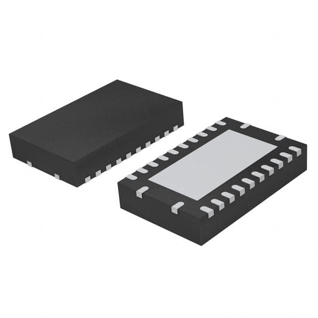
- Package: TSSOP (Thin Shrink Small Outline Package)
- Essence: High-speed CMOS technology for low power consumption and high noise immunity
- Packaging/Quantity: Tape and Reel, 2500 pieces per reel
Specifications
- Supply Voltage Range: 1.2V to 3.6V
- Logic Voltage Levels: 1.2V to 3.6V
- Input/Output Voltage Range: Ground to VCC
- Maximum Output Current: ±24mA
- Operating Temperature Range: -40°C to +125°C
- Input Capacitance: 4pF
- Propagation Delay: 4.5ns (max) at 3.3V supply, 20pF load
Detailed Pin Configuration
The 74LVC4245ABQ-Q100J has a total of 24 pins arranged in a TSSOP package. The pin configuration is as follows:
___________
   A1 |           | VCCB
   A2 |           | B1
   A3 |           | B2
   A4 |           | B3
   A5 |           | B4
   A6 |           | B5
   A7 |           | B6
   GND |           | B7
   OE  |           | B8
   DIR |           | B9
   A8  |           | B10
   A9  |           | B11
  A10  |           | B12
  A11  |           | B13
  A12  |           | B14
  VCCA |___________| B15
Functional Features
- Bi-directional voltage level translation: Allows seamless communication between devices operating at different logic levels.
- Automatic direction control: The DIR pin determines the direction of data flow, simplifying the interface design.
- Output enable control: The OE pin enables or disables the outputs, providing flexibility in controlling the bus transceiver.
Advantages and Disadvantages
Advantages: - Wide supply voltage range allows compatibility with various systems. - High-speed CMOS technology ensures fast and efficient level shifting. - Low power consumption for energy-efficient operation. - High noise immunity for reliable data transmission.
Disadvantages: - Limited maximum output current may restrict use in high-current applications. - TSSOP package may require careful handling during assembly.
Working Principles
The 74LVC4245ABQ-Q100J utilizes a combination of MOSFETs and CMOS technology to achieve bi-directional voltage level translation. It operates by monitoring the input voltage levels and automatically adjusting the output voltage levels accordingly. The DIR pin controls the direction of data flow, while the OE pin enables or disables the outputs.
Detailed Application Field Plans
The 74LVC4245ABQ-Q100J is commonly used in various applications that require voltage level translation, such as: 1. Interfacing between microcontrollers and peripheral devices operating at different logic levels. 2. Communication between different types of memory modules. 3. Level shifting in industrial automation systems. 4. Signal conversion in automotive electronics. 5. Interface design in consumer electronics.
Detailed and Complete Alternative Models
- SN74LVC4245A: Similar functionality and specifications from Texas Instruments.
- MC74LVC4245: Equivalent level shifter IC from ON Semiconductor.
- CD74LVC4245: Alternative model offered by Texas Instruments.
These alternative models provide similar voltage level translation capabilities and can be used as substitutes for the 74LVC4245ABQ-Q100J in various applications.
Word count: 496 words
Liste 10 perguntas e respostas comuns relacionadas à aplicação de 74LVC4245ABQ-Q100J em soluções técnicas
Sure! Here are 10 common questions and answers related to the application of 74LVC4245ABQ-Q100J in technical solutions:
Question: What is the 74LVC4245ABQ-Q100J?
Answer: The 74LVC4245ABQ-Q100J is a high-performance, low-voltage, octal bidirectional voltage level translator with 3-state outputs.Question: What is the operating voltage range of the 74LVC4245ABQ-Q100J?
Answer: The operating voltage range is from 1.65V to 5.5V.Question: How many bidirectional channels does the 74LVC4245ABQ-Q100J have?
Answer: It has 8 bidirectional channels.Question: What is the maximum data rate supported by the 74LVC4245ABQ-Q100J?
Answer: The maximum data rate is 400 Mbps.Question: Can the 74LVC4245ABQ-Q100J be used for level shifting between different voltage domains?
Answer: Yes, it can be used for level shifting between different voltage domains.Question: Does the 74LVC4245ABQ-Q100J support bi-directional communication?
Answer: Yes, it supports bi-directional communication.Question: What is the output drive strength of the 74LVC4245ABQ-Q100J?
Answer: The output drive strength is typically 24 mA.Question: Can the 74LVC4245ABQ-Q100J be used in automotive applications?
Answer: Yes, it is qualified for automotive applications and meets the AEC-Q100 standard.Question: What is the package type of the 74LVC4245ABQ-Q100J?
Answer: It comes in a standard SOIC-20 package.Question: Are there any special considerations when using the 74LVC4245ABQ-Q100J?
Answer: It is important to ensure that the voltage levels and timing requirements of the connected devices are compatible with the specifications of the 74LVC4245ABQ-Q100J. Additionally, proper decoupling capacitors should be used for stable operation.
Please note that these answers are general and may vary depending on the specific application and requirements.