

Veja as especificações para detalhes do produto.
74LVC16373ADL,112
Basic Information Overview
- Category: Integrated Circuit (IC)
- Use: Data storage and transfer
- Characteristics: High-speed, low-voltage, transparent latch
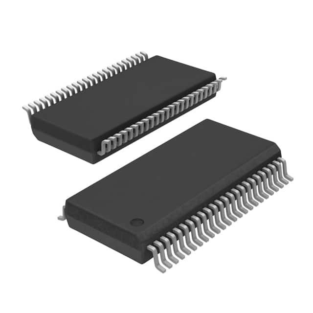
- Package: TSSOP (Thin Shrink Small Outline Package)
- Essence: Octal transparent D-type latch with 3-state outputs
- Packaging/Quantity: Tape and reel, 2500 units per reel
Specifications
- Supply Voltage Range: 1.2V to 3.6V
- Input Voltage Range: -0.5V to VCC + 0.5V
- Output Voltage Range: 0V to VCC
- Operating Temperature Range: -40°C to +125°C
- Output Drive Capability: ±24mA at 3.0V
- Propagation Delay: 4.3ns (typical) at 3.3V, 25°C
Detailed Pin Configuration
The 74LVC16373ADL,112 IC has a total of 48 pins, which are distributed as follows:
- Pin 1: GND (Ground)
- Pin 2: Q0 (Output 0)
- Pin 3: D0 (Data input 0)
- Pin 4: D1 (Data input 1)
- Pin 5: Q1 (Output 1)
- Pin 6: D2 (Data input 2)
- Pin 7: D3 (Data input 3)
- Pin 8: Q2 (Output 2)
- Pin 9: GND (Ground)
- Pin 10: Q3 (Output 3)
- Pin 11: D4 (Data input 4)
- Pin 12: D5 (Data input 5)
- Pin 13: Q4 (Output 4)
- Pin 14: D6 (Data input 6)
- Pin 15: D7 (Data input 7)
- Pin 16: Q5 (Output 5)
- Pin 17: GND (Ground)
- Pin 18: Q6 (Output 6)
- Pin 19: LE (Latch Enable)
- Pin 20: Q7 (Output 7)
- Pin 21: OE (Output Enable)
- Pin 22: GND (Ground)
- Pin 23: CP (Clock Pulse)
- Pin 24: MR (Master Reset)
- Pin 25: Qn (Output n)
- Pin 26: Dn (Data input n)
- Pins 27 to 48: GND (Ground)
Functional Features
- Octal transparent latch with 3-state outputs
- High-speed operation, suitable for high-frequency applications
- Low-voltage operation, compatible with various logic levels
- Transparent latch allows real-time data transfer
- 3-state outputs provide flexibility in connecting multiple devices
Advantages and Disadvantages
Advantages: - High-speed operation enables efficient data transfer - Low-voltage operation reduces power consumption - Transparent latch allows real-time data updates - 3-state outputs provide flexibility in bus systems
Disadvantages: - Limited output drive capability compared to some other ICs - Requires careful handling due to its small package size
Working Principles
The 74LVC16373ADL,112 is an octal transparent D-type latch with 3-state outputs. It operates based on clock pulses and latch enable signals. When the latch enable (LE) signal is high, the data inputs (D0-D7) are transferred to the corresponding outputs (Q0-Q7) in real-time. The clock pulse (CP) synchronizes this transfer. The output enable (OE) signal controls the 3-state outputs, allowing them to be either active or in a high-impedance state.
Detailed Application Field Plans
The 74LVC16373ADL,112 IC finds applications in various fields, including: 1. Microprocessor systems 2. Data storage and transfer systems 3. Communication equipment 4. Industrial automation 5. Automotive electronics
Detailed and Complete Alternative Models
Some alternative models that can be used as substitutes for the 74LVC16373ADL,112 IC are: 1. SN74LVC16373ADGGR 2. MC74LVC16373ADG 3. CD74LVC16373ADLR 4. TC74LVC16373ADGGR 5. 74LVC16373ADGG
Note: The above list is not exhaustive, and there may be other alternative models available in the market.
In conclusion, the 74LVC16373ADL,112 is a high-speed, low-voltage octal transparent latch with 3-state outputs. It is widely used in microprocessor systems,
Liste 10 perguntas e respostas comuns relacionadas à aplicação de 74LVC16373ADL,112 em soluções técnicas
Sure! Here are 10 common questions and answers related to the application of 74LVC16373ADL,112 in technical solutions:
Q: What is the function of the 74LVC16373ADL,112? A: The 74LVC16373ADL,112 is an octal transparent latch with 3-state outputs. It can store and output data from its inputs.
Q: What is the maximum operating voltage for the 74LVC16373ADL,112? A: The maximum operating voltage for the 74LVC16373ADL,112 is typically 3.6V.
Q: How many latch outputs does the 74LVC16373ADL,112 have? A: The 74LVC16373ADL,112 has 8 latch outputs.
Q: Can the 74LVC16373ADL,112 be used in both parallel and serial data transfer applications? A: Yes, the 74LVC16373ADL,112 can be used in both parallel and serial data transfer applications.
Q: What is the power supply range for the 74LVC16373ADL,112? A: The power supply range for the 74LVC16373ADL,112 is typically between 1.65V and 3.6V.
Q: Does the 74LVC16373ADL,112 support 3-state outputs? A: Yes, the 74LVC16373ADL,112 supports 3-state outputs, allowing multiple devices to share a common bus.
Q: What is the maximum data transfer rate supported by the 74LVC16373ADL,112? A: The maximum data transfer rate supported by the 74LVC16373ADL,112 is typically 400 Mbps.
Q: Can the 74LVC16373ADL,112 be used in both CMOS and TTL applications? A: Yes, the 74LVC16373ADL,112 can be used in both CMOS and TTL applications.
Q: Does the 74LVC16373ADL,112 have built-in protection against electrostatic discharge (ESD)? A: Yes, the 74LVC16373ADL,112 has built-in ESD protection to prevent damage from static electricity.
Q: What is the package type for the 74LVC16373ADL,112? A: The 74LVC16373ADL,112 is available in a TSSOP package with 48 pins.
Please note that the answers provided here are general and may vary depending on the specific datasheet and manufacturer's specifications of the 74LVC16373ADL,112.