

Veja as especificações para detalhes do produto.
Encyclopedia Entry: 74AHCT273BQ-Q100X
Product Overview
- Category: Integrated Circuit (IC)
- Use: Flip-Flop Register
- Characteristics: High-speed, Low-power, CMOS Technology
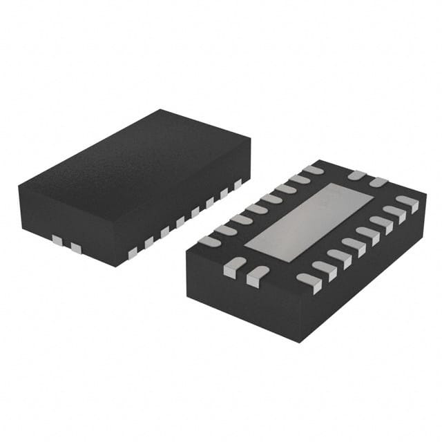
- Package: QFN (Quad Flat No-leads)
- Essence: Sequential Logic Device
- Packaging/Quantity: Tape and Reel, 2500 units per reel
Specifications
- Supply Voltage: 2.0V to 5.5V
- Input Voltage: 0V to VCC
- Output Voltage: 0V to VCC
- Operating Temperature: -40°C to +125°C
- Propagation Delay: 6 ns (typical)
- Output Drive Capability: ±8 mA
Detailed Pin Configuration
The 74AHCT273BQ-Q100X IC has a total of 20 pins, which are assigned specific functions as follows:
- CP (Clock Pulse) - Clock input for the flip-flop register.
- D0-D7 (Data Inputs) - Eight parallel data inputs.
- Q0-Q7 (Outputs) - Corresponding outputs for each data input.
- GND (Ground) - Ground reference for the IC.
- OE (Output Enable) - Output enable control input.
- MR (Master Reset) - Master reset control input.
- VCC (Power Supply) - Positive power supply voltage.
Functional Features
- The 74AHCT273BQ-Q100X is a positive-edge triggered flip-flop register.
- It can store eight bits of data using its eight data inputs (D0-D7).
- The stored data can be read from the corresponding output pins (Q0-Q7).
- The flip-flops are synchronized with the clock pulse (CP) input.
- The output enable (OE) pin allows for tri-state output control.
- The master reset (MR) pin resets all flip-flops to a known state.
Advantages and Disadvantages
Advantages: - High-speed operation, suitable for time-critical applications. - Low power consumption, ideal for battery-powered devices. - Wide operating voltage range allows for flexibility in different systems. - CMOS technology provides improved noise immunity and reliability.
Disadvantages: - Limited output drive capability may not be suitable for high-current applications. - Propagation delay of 6 ns may introduce timing issues in certain designs. - QFN package may require specialized equipment for soldering and rework.
Working Principles
The 74AHCT273BQ-Q100X operates based on positive-edge triggering. When the clock pulse (CP) transitions from low to high, the data inputs (D0-D7) are latched into their corresponding flip-flops. The stored data can then be read from the output pins (Q0-Q7). The output enable (OE) pin controls whether the outputs are active or in a high-impedance state. The master reset (MR) pin resets all flip-flops to a known state when activated.
Detailed Application Field Plans
The 74AHCT273BQ-Q100X is widely used in various digital systems and applications, including: 1. Microcontrollers and microprocessors 2. Data storage and retrieval systems 3. Communication devices and networks 4. Industrial automation and control systems 5. Automotive electronics 6. Consumer electronics
Detailed and Complete Alternative Models
- SN74HC273 - Texas Instruments
- CD74HCT273 - Texas Instruments
- MC74HCT273A - ON Semiconductor
- 74VHC273 - Fairchild Semiconductor
- 74ACT273 - NXP Semiconductors
These alternative models offer similar functionality and can be used as replacements for the 74AHCT273BQ-Q100X in various applications.
Word count: 554 words
Liste 10 perguntas e respostas comuns relacionadas à aplicação de 74AHCT273BQ-Q100X em soluções técnicas
Sure! Here are 10 common questions and answers related to the application of 74AHCT273BQ-Q100X in technical solutions:
Question: What is the function of the 74AHCT273BQ-Q100X?
Answer: The 74AHCT273BQ-Q100X is a D-type flip-flop integrated circuit that can store one bit of data.Question: What is the operating voltage range for this IC?
Answer: The 74AHCT273BQ-Q100X operates within a voltage range of 4.5V to 5.5V.Question: How many flip-flops are there in the 74AHCT273BQ-Q100X?
Answer: This IC contains 8 flip-flops, which means it can store 8 bits of data.Question: Can I use this IC in high-speed applications?
Answer: Yes, the 74AHCT273BQ-Q100X is designed for high-speed operation and can be used in such applications.Question: What is the maximum clock frequency supported by this IC?
Answer: The 74AHCT273BQ-Q100X can support clock frequencies up to 125 MHz.Question: Does this IC have any built-in latches or enable inputs?
Answer: No, the 74AHCT273BQ-Q100X does not have any built-in latches or enable inputs.Question: Can I cascade multiple 74AHCT273BQ-Q100X ICs together?
Answer: Yes, you can cascade multiple ICs to increase the number of bits that can be stored.Question: What is the power consumption of this IC?
Answer: The power consumption of the 74AHCT273BQ-Q100X is relatively low, making it suitable for battery-powered applications.Question: Can I use this IC in both rising and falling edge-triggered applications?
Answer: Yes, the 74AHCT273BQ-Q100X can be used in both rising and falling edge-triggered applications.Question: Is this IC compatible with other logic families?
Answer: Yes, the 74AHCT273BQ-Q100X is compatible with other CMOS logic families, making it versatile for various applications.
Please note that these answers are general and may vary depending on specific application requirements.