

Veja as especificações para detalhes do produto.
74AHC138BQ,115
Product Overview
- Category: Integrated Circuit (IC)
- Use: Decoding and demultiplexing
- Characteristics: High-speed operation, low power consumption
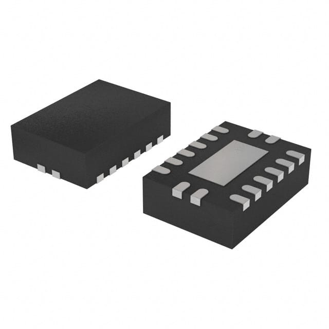
- Package: 16-pin SOIC (Small Outline Integrated Circuit)
- Essence: A 3-to-8 line decoder/demultiplexer
- Packaging/Quantity: Tape and reel, 2500 units per reel
Specifications
- Supply voltage range: 2.0V to 5.5V
- High noise immunity: VNIH = VNIL = 30% VCC (min)
- Low power consumption: ICC = 4µA (max) at TA = 25°C
- Output current: ±6mA
- Operating temperature range: -40°C to +125°C
Detailed Pin Configuration
- GND: Ground
- A0: Address input 0
- A1: Address input 1
- A2: Address input 2
- E1: Enable input 1
- E2: Enable input 2
- E3: Enable input 3
- Y0: Output 0
- Y1: Output 1
- Y2: Output 2
- Y3: Output 3
- Y4: Output 4
- Y5: Output 5
- Y6: Output 6
- Y7: Output 7
- VCC: Positive supply voltage
Functional Features
The 74AHC138BQ,115 is a high-speed CMOS decoder/demultiplexer IC. It takes three address inputs (A0, A1, A2) and three enable inputs (E1, E2, E3) to generate eight mutually exclusive outputs (Y0-Y7). The selected output is determined by the combination of address inputs and enable inputs. It operates at a wide supply voltage range and offers high noise immunity.
Advantages and Disadvantages
Advantages: - High-speed operation allows for efficient decoding and demultiplexing. - Low power consumption makes it suitable for battery-powered devices. - Wide operating temperature range enables usage in various environments. - Compact 16-pin SOIC package provides ease of integration.
Disadvantages: - Limited to 3-to-8 line decoding/demultiplexing functionality. - May require additional components for complex applications.
Working Principles
The 74AHC138BQ,115 uses a combination of address inputs and enable inputs to select one of the eight outputs. When the enable inputs are active (low), the decoder/demultiplexer decodes the binary address inputs and activates the corresponding output. The selected output remains active until the enable inputs or address inputs change.
Detailed Application Field Plans
The 74AHC138BQ,115 finds applications in various fields, including:
- Address decoding in microcontrollers and microprocessors.
- Memory selection in digital systems.
- Data routing in communication systems.
- Signal demultiplexing in audio/video equipment.
- Control signal generation in industrial automation.
Detailed and Complete Alternative Models
- 74HC138: Similar functionality with slightly different electrical characteristics.
- CD74HC138: Equivalent IC from a different manufacturer.
- SN74LS138: TTL logic family alternative with different voltage requirements.
(Note: This list is not exhaustive and other alternatives may exist.)
Word count: 420
Liste 10 perguntas e respostas comuns relacionadas à aplicação de 74AHC138BQ,115 em soluções técnicas
Sure! Here are 10 common questions and answers related to the application of 74AHC138BQ,115 in technical solutions:
Question: What is the function of the 74AHC138BQ,115?
Answer: The 74AHC138BQ,115 is a 3-to-8 line decoder/demultiplexer IC that converts binary information from three input lines into eight output lines.Question: What is the maximum operating voltage for the 74AHC138BQ,115?
Answer: The maximum operating voltage for the 74AHC138BQ,115 is 5.5V.Question: Can the 74AHC138BQ,115 be used as a multiplexer?
Answer: No, the 74AHC138BQ,115 is specifically designed as a decoder/demultiplexer and cannot be used as a multiplexer.Question: How many output lines does the 74AHC138BQ,115 have?
Answer: The 74AHC138BQ,115 has eight output lines (Y0-Y7).Question: What is the purpose of the enable pin (E) on the 74AHC138BQ,115?
Answer: The enable pin (E) is used to enable or disable the decoder/demultiplexer. When E is high, the outputs are active; when E is low, the outputs are disabled.Question: Can the 74AHC138BQ,115 be cascaded to increase the number of output lines?
Answer: Yes, multiple 74AHC138BQ,115 ICs can be cascaded together to increase the number of output lines.Question: What is the typical propagation delay of the 74AHC138BQ,115?
Answer: The typical propagation delay of the 74AHC138BQ,115 is around 6 ns.Question: Can the 74AHC138BQ,115 be used in high-speed applications?
Answer: Yes, the 74AHC138BQ,115 is designed for high-speed operation and can be used in applications with fast switching requirements.Question: What is the power supply voltage range for the 74AHC138BQ,115?
Answer: The power supply voltage range for the 74AHC138BQ,115 is from 2V to 5.5V.Question: Is the 74AHC138BQ,115 available in different package options?
Answer: Yes, the 74AHC138BQ,115 is available in various package options, such as SOIC, TSSOP, and VSSOP.
Please note that these answers are general and may vary depending on the specific datasheet and manufacturer's specifications for the 74AHC138BQ,115 IC.