

Veja as especificações para detalhes do produto.
A54SX16A-2FGG144I
Product Overview
Category
The A54SX16A-2FGG144I belongs to the category of Field Programmable Gate Arrays (FPGAs).
Use
FPGAs are integrated circuits that can be programmed and reprogrammed to perform various digital functions. The A54SX16A-2FGG144I is specifically designed for applications requiring high-performance logic integration.
Characteristics
- High-performance FPGA with 54,000 system gates
- 16,000 usable gates
- Advanced architecture for efficient logic implementation
- Low power consumption
- Fast signal processing capabilities
Package
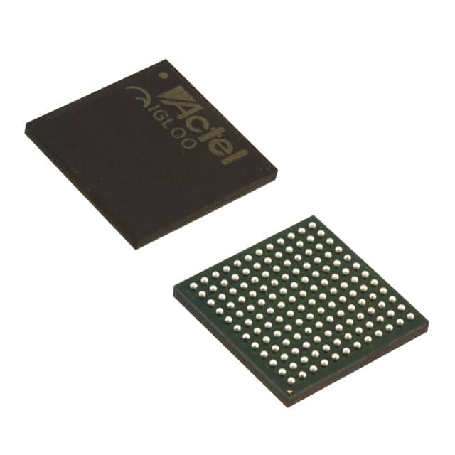
The A54SX16A-2FGG144I comes in a compact 144-pin Fine-Pitch Ball Grid Array (FBGA) package.
Essence
The essence of the A54SX16A-2FGG144I lies in its ability to provide flexible and customizable digital logic functionality through programmability.
Packaging/Quantity
The A54SX16A-2FGG144I is typically packaged individually and is available in various quantities depending on the customer's requirements.
Specifications
- System Gates: 54,000
- Usable Gates: 16,000
- Logic Cells: 1,600
- Maximum Frequency: 200 MHz
- I/O Pins: 144
- Operating Voltage: 3.3V
- Package Type: FBGA
- Temperature Range: -40°C to +85°C
Detailed Pin Configuration
The A54SX16A-2FGG144I has a total of 144 pins, which are assigned to different functions such as input/output (I/O), power supply, and configuration. The pin configuration is as follows:
- Pins 1-36: I/O pins
- Pins 37-44: Ground (GND)
- Pins 45-52: Power supply (VCC)
- Pins 53-56: Configuration pins
- Pins 57-144: I/O pins
Functional Features
High Logic Integration: The A54SX16A-2FGG144I offers a large number of usable gates, allowing for complex digital logic designs to be implemented efficiently.
Programmability: Being an FPGA, the A54SX16A-2FGG144I can be programmed and reprogrammed to adapt to changing requirements, making it highly versatile.
Low Power Consumption: The advanced architecture of the A54SX16A-2FGG144I enables it to operate with low power consumption, making it suitable for battery-powered applications.
Fast Signal Processing: With a maximum frequency of 200 MHz, the A54SX16A-2FGG144I can handle high-speed signal processing tasks effectively.
Advantages and Disadvantages
Advantages
- Flexibility: The programmable nature of FPGAs allows for customization and adaptation to specific application needs.
- High Integration: The A54SX16A-2FGG144I provides a large number of usable gates, enabling the integration of complex logic functions into a single chip.
- Fast Prototyping: FPGAs facilitate rapid prototyping by eliminating the need for custom ASIC development.
- Reusability: FPGAs can be reprogrammed multiple times, making them cost-effective for applications with evolving requirements.
Disadvantages
- Higher Cost: FPGAs tend to be more expensive compared to fixed-function integrated circuits due to their flexibility and programmability.
- Limited Performance: While FPGAs offer high logic integration, they may not match the performance of dedicated application-specific integrated circuits (ASICs) for certain specialized tasks.
- Design Complexity: Developing complex FPGA designs requires expertise in hardware description languages and digital logic design.
Working Principles
The A54SX16A-2FGG144I operates based on the principles of reconfigurable computing. It consists of an array of configurable logic blocks interconnected through programmable routing resources. The configuration data stored in the FPGA determines the functionality of each logic block and the interconnections between them. During operation, the FPGA executes the programmed logic functions by routing signals through the configured paths.
Detailed Application Field Plans
The A54SX16A-2FGG144I finds applications in various fields, including:
- Communications: Used in wireless base stations, network routers, and communication infrastructure equipment for signal processing and protocol handling.
- Industrial Automation: Employed in control systems, robotics, and machine vision applications for real-time data processing and control.
- Automotive: Utilized in automotive electronics for engine control, advanced driver-assistance systems (ADAS), and infotainment systems.
- Aerospace and Defense: Integrated into avionics systems, radar signal processing, and secure communication systems.
- Medical Devices: Applied in medical imaging, patient monitoring, and diagnostic
Liste 10 perguntas e respostas comuns relacionadas à aplicação de A54SX16A-2FGG144I em soluções técnicas
Sure! Here are 10 common questions and answers related to the application of A54SX16A-2FGG144I in technical solutions:
Q: What is the A54SX16A-2FGG144I?
- A: The A54SX16A-2FGG144I is a specific model of field-programmable gate array (FPGA) manufactured by Microsemi.
Q: What is an FPGA?
- A: FPGA stands for Field-Programmable Gate Array. It is a type of integrated circuit that can be programmed after manufacturing to perform specific functions.
Q: What are the key features of the A54SX16A-2FGG144I?
- A: The A54SX16A-2FGG144I features 54,000 system gates, 16,000 logic cells, and comes in a 144-pin Fine-Pitch Ball Grid Array (FBGA) package.
Q: What are some typical applications of the A54SX16A-2FGG144I?
- A: The A54SX16A-2FGG144I is commonly used in various technical solutions such as telecommunications, industrial automation, automotive electronics, and aerospace systems.
Q: How can I program the A54SX16A-2FGG144I?
- A: The A54SX16A-2FGG144I can be programmed using hardware description languages (HDLs) like VHDL or Verilog, which allow you to describe the desired functionality of the FPGA.
Q: Can the A54SX16A-2FGG144I be reprogrammed?
- A: Yes, FPGAs like the A54SX16A-2FGG144I are reprogrammable, which means you can change their functionality by reprogramming them with new designs.
Q: What tools do I need to program the A54SX16A-2FGG144I?
- A: To program the A54SX16A-2FGG144I, you will need a compatible development board or programmer, as well as software tools provided by Microsemi, such as Libero SoC Design Suite.
Q: Can the A54SX16A-2FGG144I interface with other components or devices?
- A: Yes, the A54SX16A-2FGG144I supports various communication interfaces like SPI, I2C, UART, and GPIOs, allowing it to interface with other components or devices in your system.
Q: What is the power consumption of the A54SX16A-2FGG144I?
- A: The power consumption of the A54SX16A-2FGG144I depends on the specific design and usage scenario. It is recommended to refer to the datasheet for detailed power specifications.
Q: Where can I find more information about the A54SX16A-2FGG144I?
- A: You can find more information about the A54SX16A-2FGG144I, including datasheets, application notes, and technical documentation, on the official Microsemi website or by contacting their support team.
Please note that the answers provided here are general and may vary depending on the specific requirements and use cases.