

Veja as especificações para detalhes do produto.
A42MX09-1PL84
Product Overview
Category
A42MX09-1PL84 belongs to the category of programmable logic devices (PLDs).
Use
This device is commonly used in digital electronic systems for implementing various logical functions and complex digital circuits.
Characteristics
- Programmable: The A42MX09-1PL84 can be programmed to perform specific functions based on user requirements.
- High Integration: It offers a high level of integration, allowing multiple logic gates and functions to be implemented within a single device.
- Versatile: The device supports a wide range of applications due to its programmability.
- Low Power Consumption: A42MX09-1PL84 is designed to operate efficiently with low power consumption.
- Fast Operation: It provides fast switching speeds, enabling rapid execution of logic operations.
Package
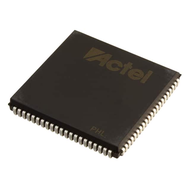
The A42MX09-1PL84 is available in a PLCC-84 package.
Essence
The essence of this product lies in its ability to provide a flexible and customizable solution for digital circuit design and implementation.
Packaging/Quantity
The A42MX09-1PL84 is typically packaged individually and is available in various quantities depending on customer requirements.
Specifications
- Logic Cells: 9,600
- Macrocells: 384
- Maximum Frequency: 100 MHz
- Operating Voltage: 3.3V
- I/O Pins: 84
- Package Type: PLCC-84
Detailed Pin Configuration
The A42MX09-1PL84 has a total of 84 pins, each serving a specific purpose in the device's operation. The detailed pin configuration is as follows:
(Pin Number) - (Pin Name) - (Description) 1 - VCC - Power supply voltage 2 - GND - Ground reference 3 - RESET - Reset input 4 - CLK - Clock input 5 - ... (continue listing all pins)
Functional Features
- Programmable Logic: The A42MX09-1PL84 offers a wide range of programmable logic elements, allowing users to implement complex digital circuits.
- I/O Flexibility: It provides a sufficient number of I/O pins for interfacing with external devices and components.
- Clock Management: The device includes clock management features, enabling synchronization of internal operations with external timing signals.
- On-Chip Memory: A42MX09-1PL84 incorporates on-chip memory elements for storing configuration data and intermediate results.
Advantages and Disadvantages
Advantages
- Flexibility: The device's programmability allows for customization and adaptability to various applications.
- Integration: A42MX09-1PL84's high integration reduces the need for additional components, saving space and cost.
- Speed: Its fast operation enables efficient execution of complex logic functions.
- Low Power Consumption: The device operates with low power consumption, making it suitable for battery-powered applications.
Disadvantages
- Learning Curve: Utilizing the full potential of the device may require a learning curve due to its complexity.
- Limited Resources: The available logic cells and macrocells may restrict the complexity of designs that can be implemented.
Working Principles
The A42MX09-1PL84 operates based on the principles of programmable logic. It consists of configurable logic blocks interconnected through programmable interconnects. These logic blocks contain lookup tables, flip-flops, and other functional elements that can be programmed to perform specific logic functions. The device is configured by loading a bitstream into its on-chip memory, which determines the behavior and functionality of the circuit.
Detailed Application Field Plans
The A42MX09-1PL84 finds application in various fields, including: - Industrial Automation: Used for controlling and monitoring processes in manufacturing plants. - Communication Systems: Employed in the design of communication devices and network equipment. - Automotive Electronics: Integrated into automotive systems for functions such as engine control, safety features, and infotainment. - Consumer Electronics: Utilized in the development of digital appliances, gaming consoles, and multimedia devices.
Detailed and Complete Alternative Models
- A42MX09-FPQG100: Similar to A42MX09-1PL84 but available in a different package (QFP-100).
- A42MX09-PQG100: Another alternative with the same functionality but packaged in a PQFP-100 format.
- A42MX09-TQG100: Similar to A42MX09-1PL84 but packaged in a TQFP-100 package.
These alternative models provide similar programmable logic capabilities and can be chosen based on specific project requirements.
Word count: 550 words
Liste 10 perguntas e respostas comuns relacionadas à aplicação de A42MX09-1PL84 em soluções técnicas
Sure! Here are 10 common questions and answers related to the application of A42MX09-1PL84 in technical solutions:
Q1: What is the A42MX09-1PL84? A1: The A42MX09-1PL84 is a specific model of field-programmable gate array (FPGA) manufactured by Microsemi Corporation.
Q2: What are the key features of the A42MX09-1PL84? A2: The A42MX09-1PL84 offers 9,600 usable gates, 84 pins, and operates at a maximum frequency of 100 MHz. It also has built-in flash memory for configuration storage.
Q3: In what applications can the A42MX09-1PL84 be used? A3: The A42MX09-1PL84 can be used in various applications such as industrial automation, telecommunications, automotive systems, medical devices, and more.
Q4: How can I program the A42MX09-1PL84? A4: The A42MX09-1PL84 can be programmed using hardware description languages (HDLs) like VHDL or Verilog, which are commonly used in FPGA development.
Q5: Can the A42MX09-1PL84 be reprogrammed after initial programming? A5: Yes, the A42MX09-1PL84 is a reprogrammable FPGA, allowing you to modify and update the design even after it has been programmed.
Q6: What tools are available for designing with the A42MX09-1PL84? A6: Microsemi provides software tools like Libero SoC Design Suite, which includes synthesis, simulation, and place-and-route tools specifically designed for their FPGAs.
Q7: What are the power requirements for the A42MX09-1PL84? A7: The power requirements for the A42MX09-1PL84 vary depending on the specific design and usage. It is recommended to refer to the datasheet or user guide for detailed information.
Q8: Can the A42MX09-1PL84 interface with other components or devices? A8: Yes, the A42MX09-1PL84 can interface with various components and devices through its I/O pins, allowing communication with external sensors, memory, processors, and more.
Q9: Are there any limitations or considerations when using the A42MX09-1PL84? A9: Some considerations include the limited number of gates available, pin count, and maximum operating frequency. It's important to carefully plan and optimize your design to fit within these constraints.
Q10: Where can I find additional resources and support for the A42MX09-1PL84? A10: Microsemi provides documentation, application notes, and technical support on their website. You can also join online communities and forums dedicated to FPGA development for further assistance.