

Veja as especificações para detalhes do produto.
ATF750C-15GM/883
Product Overview
Category
ATF750C-15GM/883 belongs to the category of programmable logic devices (PLDs).
Use
This product is commonly used in digital circuit design and implementation. It provides a flexible and customizable solution for various applications.
Characteristics
- Programmable: The ATF750C-15GM/883 can be programmed to perform specific functions according to the user's requirements.
- High-speed operation: It operates at a speed of 15 nanoseconds, enabling efficient data processing.
- Low power consumption: This PLD is designed to consume minimal power, making it suitable for battery-powered devices.
- Durable package: The ATF750C-15GM/883 is housed in a rugged package that ensures protection against environmental factors and mechanical stress.
- Versatile: It supports a wide range of applications due to its programmability.
Package and Quantity
The ATF750C-15GM/883 is available in a ceramic package. Each package contains one unit of the PLD.
Specifications
- Operating Voltage: 5V
- Maximum Operating Frequency: 66 MHz
- Number of Inputs: 32
- Number of Outputs: 16
- Programmable Logic Cells: 750
- Operating Temperature Range: -55°C to +125°C
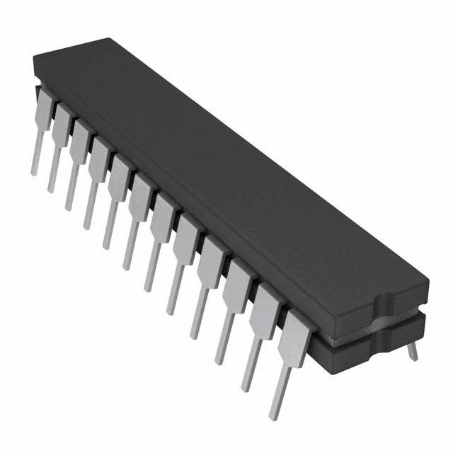
Pin Configuration
The ATF750C-15GM/883 has a total of 44 pins. The pin configuration is as follows:
- VCC
- GND
- I/O0
- I/O1
- I/O2
- I/O3
- I/O4
- I/O5
- I/O6
- I/O7
- I/O8
- I/O9
- I/O10
- I/O11
- I/O12
- I/O13
- I/O14
- I/O15
- CLK
- CE
- OE
- WE
- RESET
- JTAG_TDI
- JTAG_TMS
- JTAG_TCK
- JTAG_TDO
- NC
- NC
- NC
- NC
- NC
- NC
- NC
- NC
- NC
- NC
- NC
- NC
- NC
- NC
- NC
- NC
- NC
Functional Features
- Programmability: The ATF750C-15GM/883 can be programmed using industry-standard hardware description languages (HDL) or software tools.
- Logic Functions: It supports a variety of logic functions, including AND, OR, XOR, and more.
- Macrocells: The PLD contains multiple macrocells that can be configured to perform complex operations.
- Interconnectivity: The device allows for flexible interconnection between its internal components, enabling the creation of intricate digital circuits.
Advantages and Disadvantages
Advantages
- Flexibility: The ATF750C-15GM/883 offers great flexibility in designing digital circuits, allowing for customization according to specific requirements.
- High-speed operation: With a speed of 15 nanoseconds, it enables efficient data processing.
- Low power consumption: The PLD is designed to consume minimal power, making it suitable for battery-powered devices.
Disadvantages
- Limited capacity: The ATF750C-15GM/883 has a limited number of programmable logic cells, which may restrict the complexity of designs it can accommodate.
- Programming complexity: Programming the PLD requires expertise in HDL or dedicated software tools, which may pose a challenge for beginners.
Working Principles
The ATF750C-15GM/883 operates based on the principles of programmable logic. It consists of configurable logic blocks (CLBs) that can be programmed to perform specific functions. These CLBs are interconnected through programmable interconnects, allowing for the creation of complex digital circuits. The PLD's functionality is determined by the programming instructions provided by the user.
Application Field Plans
The ATF750C-15GM/883 finds applications in various fields, including: 1. Telecommunications: Used in the design of communication systems and network equipment. 2. Industrial Automation: Employed in control systems and process automation. 3. Automotive Electronics: Integrated into automotive control units and electronic systems. 4. Consumer Electronics: Utilized in devices such as gaming consoles, home appliances, and audio/video equipment. 5. Medical Devices: Incorporated into medical equipment for data processing and control.
Alternative Models
- ATF1502ASV-15JC44: A similar PLD with higher capacity and additional features.
- ATF16V8BQL-15PU: A low-power PL
Liste 10 perguntas e respostas comuns relacionadas à aplicação de ATF750C-15GM/883 em soluções técnicas
What is the operating temperature range of ATF750C-15GM/883?
- The operating temperature range of ATF750C-15GM/883 is -55°C to 125°C.What is the maximum clock frequency supported by ATF750C-15GM/883?
- ATF750C-15GM/883 supports a maximum clock frequency of 15MHz.Can ATF750C-15GM/883 be used in automotive applications?
- Yes, ATF750C-15GM/883 is suitable for automotive applications as it meets the necessary standards and requirements.What is the power supply voltage range for ATF750C-15GM/883?
- The power supply voltage range for ATF750C-15GM/883 is typically 4.5V to 5.5V.Does ATF750C-15GM/883 support in-system programming (ISP)?
- Yes, ATF750C-15GM/883 supports in-system programming for convenient device configuration.What are the typical applications of ATF750C-15GM/883?
- Typical applications of ATF750C-15GM/883 include memory expansion, address decoding, and bus interface control in various electronic systems.Is ATF750C-15GM/883 compatible with standard TTL input levels?
- Yes, ATF750C-15GM/883 is compatible with standard TTL input levels, making it versatile for integration into different designs.What is the package type of ATF750C-15GM/883?
- ATF750C-15GM/883 is available in a 28-pin ceramic DIP (Dual In-line Package) for robust and reliable mounting.Can ATF750C-15GM/883 be used in military-grade applications?
- Yes, ATF750C-15GM/883 is designed to meet military-grade specifications and can be used in demanding military applications.Are there any specific design considerations when using ATF750C-15GM/883 in high-speed data processing systems?
- When integrating ATF750C-15GM/883 into high-speed data processing systems, careful attention should be paid to signal integrity, noise immunity, and proper PCB layout to ensure optimal performance.