

Veja as especificações para detalhes do produto.
ATF1504AS-15JI84
Product Overview
Category
ATF1504AS-15JI84 belongs to the category of programmable logic devices (PLDs).
Use
This product is primarily used in digital circuit design and implementation. It provides a flexible and customizable solution for various applications.
Characteristics
- Programmable: The ATF1504AS-15JI84 can be programmed to perform specific functions based on the user's requirements.
- High Integration: It integrates multiple logic gates, flip-flops, and other components into a single device, reducing the need for external components.
- Versatile: The device supports a wide range of applications due to its programmability.
- Low Power Consumption: The ATF1504AS-15JI84 is designed to operate efficiently with low power consumption.
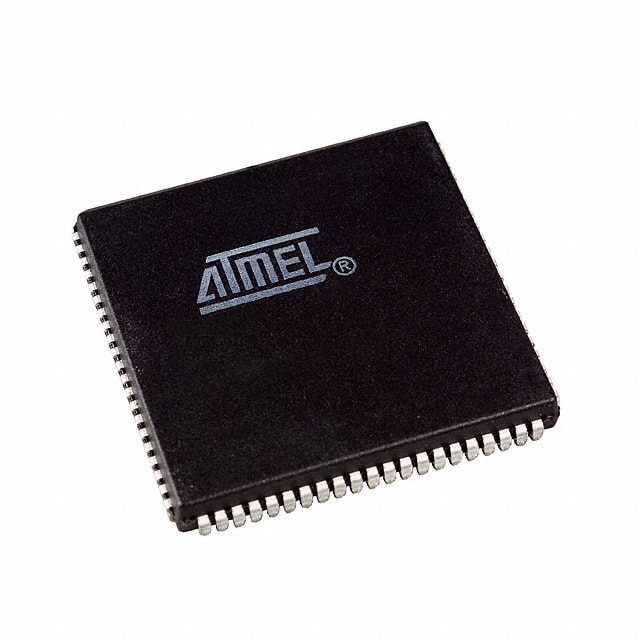
- Compact Package: It comes in a 84-pin JI package, which ensures easy integration into circuit boards.
Packaging/Quantity
The ATF1504AS-15JI84 is typically packaged individually and is available in various quantities depending on the manufacturer's specifications.
Specifications
- Device Type: Programmable Logic Device (PLD)
- Model Number: ATF1504AS-15JI84
- Package Type: 84-pin JI package
- Operating Voltage: 3.3V
- Maximum Operating Frequency: 15 MHz
- Programmable Logic Cells: 1500
- I/O Pins: 68
- On-Chip Memory: 64K bits
- Programmable Interconnects: Yes
- Clock Management: Yes
- Power Consumption: Low
Detailed Pin Configuration
The ATF1504AS-15JI84 has a total of 84 pins. The pin configuration is as follows:
- VCCIO
- GND
- IO_0
- IO_1
- IO_2
- IO_3
- IO_4
- IO_5
- IO_6
- IO_7
- IO_8
- IO_9
- IO_10
- IO_11
- IO_12
- IO_13
- IO_14
- IO_15
- IO_16
- IO_17
- IO_18
- IO_19
- IO_20
- IO_21
- IO_22
- IO_23
- IO_24
- IO_25
- IO_26
- IO_27
- IO_28
- IO_29
- IO_30
- IO_31
- IO_32
- IO_33
- IO_34
- IO_35
- IO_36
- IO_37
- IO_38
- IO_39
- IO_40
- IO_41
- IO_42
- IO_43
- IO_44
- IO_45
- IO_46
- IO_47
- IO_48
- IO_49
- IO_50
- IO_51
- IO_52
- IO_53
- IO_54
- IO_55
- IO_56
- IO_57
- IO_58
- IO_59
- IO_60
- IO_61
- IO_62
- IO_63
- TCK
- TMS
- TDI
- TDO
- GND
- VCCIO
- GND
- VCCIO
- GND
- VCCIO
- GND
- VCCIO
- GND
- VCCIO
- GND
- VCCIO
- GND
- VCCIO
Functional Features
- Programmability: The ATF1504AS-15JI84 can be programmed to implement various logic functions.
- High Integration: It integrates a large number of logic cells and I/O pins, allowing for complex circuit designs.
- Clock Management: The device supports clock management features, enabling synchronization with other components.
- On-Chip Memory: With 64K bits of on-chip memory, the ATF1504AS-15JI84 can store data and configuration information.
Advantages and Disadvantages
Advantages
- Flexibility: The ATF1504AS-15JI84 offers flexibility in designing and implementing digital circuits.
- Cost-Effective: By eliminating the need for multiple discrete components, it reduces overall system
Liste 10 perguntas e respostas comuns relacionadas à aplicação de ATF1504AS-15JI84 em soluções técnicas
Sure! Here are 10 common questions and answers related to the application of ATF1504AS-15JI84 in technical solutions:
Q: What is ATF1504AS-15JI84? A: ATF1504AS-15JI84 is a specific model of Field-Programmable Gate Array (FPGA) manufactured by Microchip Technology.
Q: What are the key features of ATF1504AS-15JI84? A: Some key features of ATF1504AS-15JI84 include 1500 usable gates, 84-pin PLCC package, 15ns maximum propagation delay, and 5V operation.
Q: How can ATF1504AS-15JI84 be used in technical solutions? A: ATF1504AS-15JI84 can be used for various applications such as digital signal processing, data acquisition, control systems, and communication interfaces.
Q: What programming languages can be used with ATF1504AS-15JI84? A: ATF1504AS-15JI84 can be programmed using Hardware Description Languages (HDLs) like VHDL or Verilog.
Q: Can ATF1504AS-15JI84 be reprogrammed after initial configuration? A: Yes, ATF1504AS-15JI84 is a reprogrammable FPGA, allowing for multiple configurations during its lifetime.
Q: What tools are required to program ATF1504AS-15JI84? A: To program ATF1504AS-15JI84, you will need a compatible programmer, such as a USB Blaster or ByteBlasterMV, along with the appropriate software like Quartus Prime.
Q: What is the power supply requirement for ATF1504AS-15JI84? A: ATF1504AS-15JI84 operates on a 5V power supply.
Q: Can ATF1504AS-15JI84 interface with other components or devices? A: Yes, ATF1504AS-15JI84 can interface with various components and devices through its I/O pins, allowing for communication and integration within a larger system.
Q: Are there any limitations or considerations when using ATF1504AS-15JI84? A: Some considerations include the limited number of usable gates, the need for external programming hardware, and the requirement for proper power supply and cooling.
Q: Where can I find more information about ATF1504AS-15JI84? A: You can refer to the datasheet and technical documentation provided by Microchip Technology for detailed information about ATF1504AS-15JI84, including its specifications, pinout, and application examples.
Please note that these answers are general and may vary depending on specific requirements and use cases. It's always recommended to consult the manufacturer's documentation for accurate and up-to-date information.