

Veja as especificações para detalhes do produto.
DG509ADY+T
Product Overview
- Category: Integrated Circuit
- Use: Digital Multiplexer
- Characteristics: High-speed, Low-power, 8:1 Multiplexer
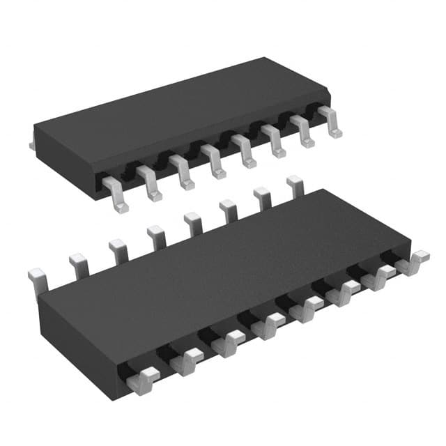
- Package: SOIC (Small Outline Integrated Circuit)
- Essence: A multiplexer is a device that selects one of several input signals and forwards it to a single output line.
- Packaging/Quantity: Available in reels of 2500 units
Specifications
- Supply Voltage: 2V to 6V
- Input Voltage: 0V to Vcc
- Operating Temperature: -40°C to +85°C
- Propagation Delay: 5ns (typical)
- Output Current: ±25mA
- Input Capacitance: 3pF (typical)
Detailed Pin Configuration
The DG509ADY+T has a total of 16 pins. The pin configuration is as follows:
- A0 - Input A0
- A1 - Input A1
- A2 - Input A2
- A3 - Input A3
- A4 - Input A4
- A5 - Input A5
- A6 - Input A6
- A7 - Input A7
- GND - Ground
- EN - Enable Input
- S0 - Select Input 0
- S1 - Select Input 1
- S2 - Select Input 2
- S3 - Select Input 3
- Y - Output
- VCC - Supply Voltage
Functional Features
- High-speed operation allows for efficient signal switching.
- Low-power consumption makes it suitable for battery-powered devices.
- Wide operating voltage range provides flexibility in various applications.
- Enables selection of one out of eight input signals.
- Output current capability allows for driving external loads.
Advantages and Disadvantages
Advantages: - High-speed operation ensures minimal signal delay. - Low-power consumption extends battery life in portable devices. - Wide operating voltage range enhances versatility. - Compact SOIC package saves board space. - Can handle moderate output currents.
Disadvantages: - Limited to 8:1 multiplexing, may not be suitable for applications requiring higher channel counts. - Not suitable for high-frequency applications due to limited bandwidth.
Working Principles
The DG509ADY+T is a digital multiplexer that operates by selecting one of the eight input signals based on the select inputs (S0-S3). The enable input (EN) controls the output state. When EN is high, the selected input is forwarded to the output pin (Y). When EN is low, the output is in a high-impedance state.
Detailed Application Field Plans
The DG509ADY+T can be used in various applications, including but not limited to:
- Data communication systems
- Analog-to-digital converters
- Digital audio equipment
- Industrial control systems
- Test and measurement instruments
Detailed and Complete Alternative Models
- CD4051B - 8-Channel Analog Multiplexer/Demultiplexer
- SN74HC151 - 8-Input Multiplexer
- MC14051B - 8-Channel Analog Multiplexer/Demultiplexer
- MAX4617 - Low-Voltage, Single-Supply, SPST Analog Switch
These alternative models offer similar functionality and can be considered as alternatives to the DG509ADY+T depending on specific requirements.
Word count: 431 words
Liste 10 perguntas e respostas comuns relacionadas à aplicação de DG509ADY+T em soluções técnicas
Sure! Here are 10 common questions and answers related to the application of DG509ADY+T in technical solutions:
Q: What is DG509ADY+T? A: DG509ADY+T is a specific model of integrated circuit (IC) used for various technical applications.
Q: What are the key features of DG509ADY+T? A: Some key features of DG509ADY+T include multiple analog switches, low power consumption, and compatibility with different voltage levels.
Q: How can DG509ADY+T be used in technical solutions? A: DG509ADY+T can be used as a signal switch or multiplexer in electronic circuits, allowing for the routing of signals between different components.
Q: What is the voltage range supported by DG509ADY+T? A: DG509ADY+T supports a wide voltage range, typically from -5V to +5V, making it suitable for both analog and digital applications.
Q: Can DG509ADY+T handle high-frequency signals? A: Yes, DG509ADY+T is designed to handle high-frequency signals, making it suitable for applications that require fast switching.
Q: Is DG509ADY+T compatible with different logic families? A: Yes, DG509ADY+T is compatible with various logic families such as TTL, CMOS, and LVCMOS, ensuring its versatility in different systems.
Q: What is the power supply requirement for DG509ADY+T? A: DG509ADY+T typically operates on a single power supply ranging from +2.7V to +12V, depending on the specific application requirements.
Q: Can DG509ADY+T be used in battery-powered devices? A: Yes, DG509ADY+T's low power consumption makes it suitable for battery-powered devices where energy efficiency is crucial.
Q: Are there any specific precautions to consider when using DG509ADY+T? A: It is important to ensure that the voltage levels and signal characteristics are within the specified limits of DG509ADY+T to avoid damage or malfunction.
Q: Where can I find more information about DG509ADY+T and its application notes? A: You can refer to the manufacturer's datasheet and application notes for detailed information on DG509ADY+T, including circuit examples and guidelines for usage.
Please note that the answers provided here are general and may vary depending on the specific requirements and context of the technical solution.