

Veja as especificações para detalhes do produto.
LTC6912IDE-1#PBF
Product Overview
Category
The LTC6912IDE-1#PBF belongs to the category of integrated circuits (ICs) and specifically falls under the operational amplifier (op-amp) family.
Use
This product is primarily used in electronic circuits for amplification and signal conditioning purposes. It is commonly employed in various applications such as audio systems, instrumentation, communication devices, and control systems.
Characteristics
- High gain: The LTC6912IDE-1#PBF offers a high voltage gain, allowing for accurate amplification of weak signals.
- Low noise: This IC has low input-referred noise, ensuring minimal interference with the desired signal.
- Wide bandwidth: With a wide frequency response range, it can handle signals across a broad spectrum.
- Rail-to-rail inputs and outputs: The op-amp supports input and output voltages that can reach the power supply rails, maximizing dynamic range.
- Low power consumption: The LTC6912IDE-1#PBF operates efficiently, consuming minimal power during operation.
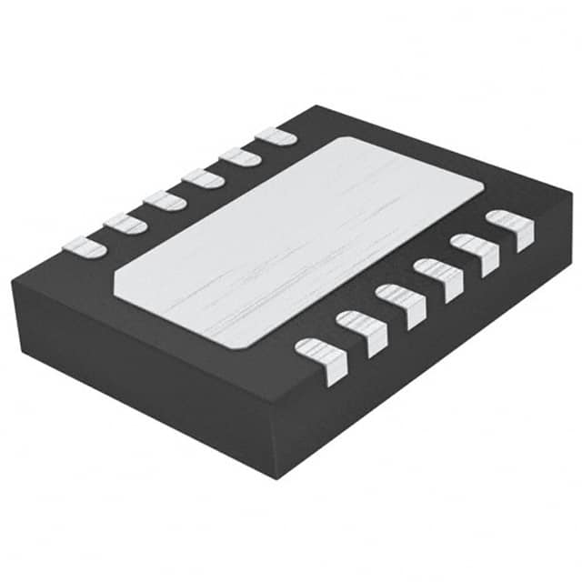
Package
The LTC6912IDE-1#PBF comes in a standard 16-pin plastic dual in-line package (PDIP), which provides ease of integration into circuit boards. The package ensures mechanical stability and protection for the internal components.
Essence
The essence of the LTC6912IDE-1#PBF lies in its ability to amplify and condition electrical signals accurately and reliably. It enhances the performance of electronic systems by providing precise signal processing capabilities.
Packaging/Quantity
The LTC6912IDE-1#PBF is typically available in reels or tubes, containing a specific quantity of ICs per packaging unit. The exact quantity may vary depending on the manufacturer's specifications and customer requirements.
Specifications
- Supply Voltage Range: ±2.5V to ±18V
- Input Offset Voltage: ±0.5mV (maximum)
- Gain Bandwidth Product: 10MHz
- Input Bias Current: ±1nA (maximum)
- Output Current: ±20mA (maximum)
- Operating Temperature Range: -40°C to +85°C
Detailed Pin Configuration
The LTC6912IDE-1#PBF features a 16-pin configuration, with each pin serving a specific function. The following table provides a detailed pin description:
| Pin Number | Pin Name | Function | |------------|----------|----------| | 1 | IN- | Inverting input | | 2 | V- | Negative power supply | | 3 | OUT | Output | | 4 | V+ | Positive power supply | | 5 | NC | No connection | | 6 | IN+ | Non-inverting input | | 7 | NC | No connection | | 8 | NC | No connection | | 9 | NC | No connection | | 10 | NC | No connection | | 11 | NC | No connection | | 12 | NC | No connection | | 13 | NC | No connection | | 14 | NC | No connection | | 15 | NC | No connection | | 16 | NC | No connection |
Functional Features
The LTC6912IDE-1#PBF offers several functional features that contribute to its versatility and performance:
- High gain: The op-amp provides a high voltage gain, allowing for precise amplification of weak signals.
- Rail-to-rail inputs and outputs: It supports input and output voltages that can reach the power supply rails, enabling maximum dynamic range.
- Low noise: The IC has low input-referred noise, ensuring minimal interference with the desired signal.
- Wide bandwidth: With a wide frequency response range, it can handle signals across a broad spectrum.
- Low power consumption: The LTC6912IDE-1#PBF operates efficiently, consuming minimal power during operation.
Advantages and Disadvantages
Advantages
- High gain for accurate signal amplification
- Rail-to-rail inputs and outputs for maximum dynamic range
- Low noise for minimal interference
- Wide bandwidth for handling various frequencies
- Low power consumption for efficient operation
Disadvantages
- Limited pin configuration options
- May require additional external components for specific applications
Working Principles
The LTC6912IDE-1#PBF operates based on the principles of operational amplifiers. It utilizes differential input stages, feedback networks, and output stages to amplify and condition electrical signals. By adjusting the gain and applying appropriate feedback, it can accurately process and amplify weak input signals to desired levels.
Detailed Application Field Plans
The LTC6912IDE-1#PBF finds application in various fields, including:
- Audio Systems:
Liste 10 perguntas e respostas comuns relacionadas à aplicação de LTC6912IDE-1#PBF em soluções técnicas
What is the maximum supply voltage for LTC6912IDE-1#PBF?
- The maximum supply voltage for LTC6912IDE-1#PBF is 36V.What is the typical input bias current of LTC6912IDE-1#PBF?
- The typical input bias current of LTC6912IDE-1#PBF is 1nA.Can LTC6912IDE-1#PBF be used in high-temperature environments?
- Yes, LTC6912IDE-1#PBF is designed to operate in high-temperature environments with a temperature range of -40°C to 125°C.What is the gain bandwidth product of LTC6912IDE-1#PBF?
- The gain bandwidth product of LTC6912IDE-1#PBF is 10MHz.Is LTC6912IDE-1#PBF suitable for battery-powered applications?
- Yes, LTC6912IDE-1#PBF is suitable for battery-powered applications due to its low power consumption.Can LTC6912IDE-1#PBF be used in precision instrumentation applications?
- Yes, LTC6912IDE-1#PBF is suitable for precision instrumentation applications due to its low offset voltage and low noise.What is the common-mode rejection ratio (CMRR) of LTC6912IDE-1#PBF?
- The CMRR of LTC6912IDE-1#PBF is typically 100dB.Does LTC6912IDE-1#PBF require external compensation?
- No, LTC6912IDE-1#PBF does not require external compensation.Can LTC6912IDE-1#PBF be used in single-supply applications?
- Yes, LTC6912IDE-1#PBF can be used in single-supply applications with proper biasing.What is the package type of LTC6912IDE-1#PBF?
- LTC6912IDE-1#PBF is available in a 16-lead plastic DFN package.