

Veja as especificações para detalhes do produto.
LTC6255CDC#TRMPBF
Product Overview
Category: Integrated Circuit (IC)
Use: The LTC6255CDC#TRMPBF is a high-speed operational amplifier designed for use in various electronic applications. It provides excellent performance and versatility, making it suitable for a wide range of uses.
Characteristics: - High speed: The LTC6255CDC#TRMPBF offers fast response times, allowing for quick signal processing. - Low noise: It has low input and output noise levels, ensuring accurate signal amplification. - Wide supply voltage range: The operational amplifier can operate from a wide range of supply voltages, providing flexibility in different applications. - Rail-to-rail inputs and outputs: The LTC6255CDC#TRMPBF supports rail-to-rail input and output voltage ranges, enabling maximum utilization of the available dynamic range. - Low power consumption: It consumes minimal power, making it suitable for battery-powered devices.
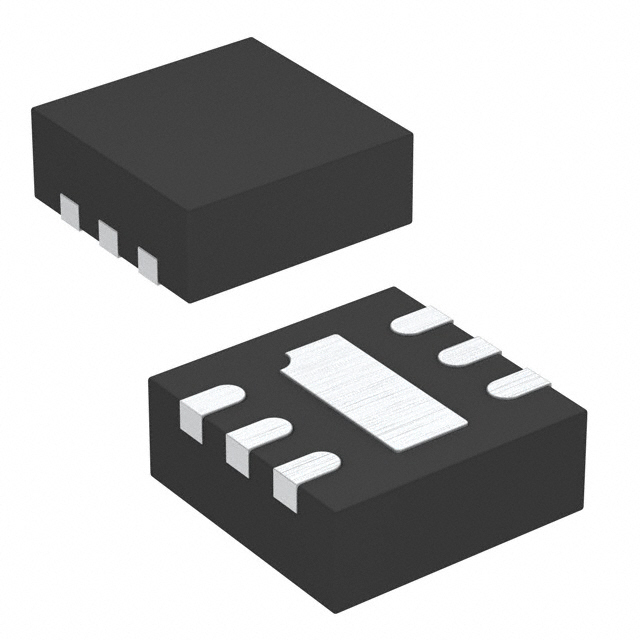
Package: The LTC6255CDC#TRMPBF comes in a small 6-pin DFN (Dual Flat No-Lead) package, which allows for easy integration into compact circuit designs.
Essence: The essence of the LTC6255CDC#TRMPBF lies in its ability to provide high-speed and low-noise amplification in a compact package, making it an ideal choice for applications that require precision and efficiency.
Packaging/Quantity: The LTC6255CDC#TRMPBF is typically sold in reels or tubes, with a quantity of 2500 units per reel/tube.
Specifications
- Supply Voltage Range: 2.7V to 5.5V
- Input Offset Voltage: ±1mV (maximum)
- Gain Bandwidth Product: 100MHz
- Slew Rate: 300V/µs
- Input Bias Current: ±20nA (maximum)
- Operating Temperature Range: -40°C to 125°C
Detailed Pin Configuration
The LTC6255CDC#TRMPBF has the following pin configuration:
- V+ (Positive Supply Voltage)
- IN- (Inverting Input)
- IN+ (Non-Inverting Input)
- V- (Negative Supply Voltage)
- OUT (Output)
- NC (No Connection)
Functional Features
- High-speed amplification: The LTC6255CDC#TRMPBF can amplify signals with high bandwidth, allowing for accurate and fast signal processing.
- Low noise operation: It provides low input and output noise levels, ensuring minimal distortion and interference in the amplified signals.
- Rail-to-rail inputs and outputs: The operational amplifier supports input and output voltage ranges that cover the entire supply voltage range, maximizing the dynamic range of the signals.
- Low power consumption: The LTC6255CDC#TRMPBF consumes minimal power, making it suitable for battery-powered applications.
- Stable operation: It offers excellent stability and performance over a wide range of operating conditions.
Advantages and Disadvantages
Advantages: - High-speed performance - Low noise operation - Wide supply voltage range - Rail-to-rail inputs and outputs - Low power consumption
Disadvantages: - Limited number of pins for additional functionality - Not suitable for high-voltage applications
Working Principles
The LTC6255CDC#TRMPBF operates based on the principles of operational amplifiers. It amplifies the difference between the voltages at its inverting and non-inverting inputs, producing an amplified output signal. The high-speed and low-noise characteristics of this operational amplifier are achieved through careful design and optimization of its internal circuitry.
Detailed Application Field Plans
The LTC6255CDC#TRMPBF finds applications in various fields, including: 1. Audio amplification: It can be used in audio equipment to amplify low-level signals with high fidelity. 2. Instrumentation and measurement: The operational amplifier is suitable for precision measurement applications that require accurate signal amplification. 3. Communications: It can be utilized in communication systems for signal conditioning and amplification purposes. 4. Sensor interfaces: The LTC6255CDC#TRMPBF can interface with sensors to amplify their output signals for further processing.
Detailed and Complete Alternative Models
- AD8065: This operational amplifier offers similar high-speed performance and low noise characteristics.
- MAX4239: It provides rail-to-rail inputs and outputs, making it suitable for applications requiring maximum dynamic range.
- OPA2188: This operational amplifier offers low power consumption and wide supply voltage range, similar to the LTC6255CDC#TRMPBF.
These alternative models can be considered based on specific application requirements and design constraints.
Word count: 550 words
Liste 10 perguntas e respostas comuns relacionadas à aplicação de LTC6255CDC#TRMPBF em soluções técnicas
Sure! Here are 10 common questions and answers related to the application of LTC6255CDC#TRMPBF in technical solutions:
Q: What is LTC6255CDC#TRMPBF? A: LTC6255CDC#TRMPBF is a high-speed, low-power operational amplifier (op-amp) manufactured by Linear Technology (now part of Analog Devices). It is commonly used in various technical applications.
Q: What are the key features of LTC6255CDC#TRMPBF? A: Some key features of LTC6255CDC#TRMPBF include a wide supply voltage range, low input bias current, low input offset voltage, high slew rate, and low quiescent current.
Q: What are the typical applications of LTC6255CDC#TRMPBF? A: LTC6255CDC#TRMPBF is commonly used in applications such as active filters, data acquisition systems, instrumentation amplifiers, signal conditioning circuits, and other high-speed, low-power applications.
Q: What is the maximum supply voltage for LTC6255CDC#TRMPBF? A: The maximum supply voltage for LTC6255CDC#TRMPBF is typically ±15V, but it can handle up to ±18V in certain conditions.
Q: What is the input bias current of LTC6255CDC#TRMPBF? A: The input bias current of LTC6255CDC#TRMPBF is typically very low, around 1nA.
Q: What is the input offset voltage of LTC6255CDC#TRMPBF? A: The input offset voltage of LTC6255CDC#TRMPBF is typically very low, around 300µV.
Q: What is the bandwidth of LTC6255CDC#TRMPBF? A: The bandwidth of LTC6255CDC#TRMPBF is typically around 200MHz.
Q: What is the quiescent current consumption of LTC6255CDC#TRMPBF? A: The quiescent current consumption of LTC6255CDC#TRMPBF is typically very low, around 1.3mA.
Q: Can LTC6255CDC#TRMPBF operate with a single supply voltage? A: Yes, LTC6255CDC#TRMPBF can operate with a single supply voltage as low as 2.7V, making it suitable for battery-powered applications.
Q: Is LTC6255CDC#TRMPBF available in different package options? A: Yes, LTC6255CDC#TRMPBF is available in various package options, including the CDC and DFN packages, providing flexibility for different PCB layouts and space constraints.
Please note that the answers provided here are general and may vary depending on specific datasheet specifications or application requirements.