

Veja as especificações para detalhes do produto.
LTC4302CMS-1#PBF
Product Overview
Category
LTC4302CMS-1#PBF belongs to the category of electronic components, specifically integrated circuits (ICs).
Use
This product is commonly used in electronic systems for level shifting and bus buffering applications.
Characteristics
- Level shifting capability
- Bus buffering functionality
- Low voltage operation
- Small form factor
- High reliability
Package
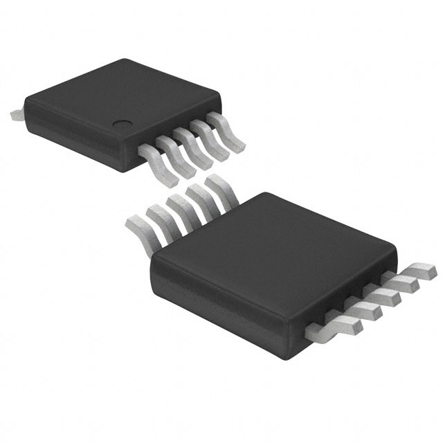
LTC4302CMS-1#PBF is available in a miniature surface-mount package, typically a 10-pin MSOP (Mini Small Outline Package).
Essence
The essence of LTC4302CMS-1#PBF lies in its ability to provide level shifting and bus buffering functions, enabling seamless communication between devices operating at different voltage levels.
Packaging/Quantity
This product is usually packaged in reels or tubes, with a typical quantity of 250 units per reel/tube.
Specifications
- Supply Voltage: 1.65V to 5.5V
- Operating Temperature Range: -40°C to 85°C
- Maximum Data Rate: 400kHz
- Quiescent Current: 0.8μA (typical)
- Number of Pins: 10
- Input/Output Logic Compatibility: CMOS/TTL
Detailed Pin Configuration
- SDA (Serial Data Input/Output)
- SCL (Serial Clock Input)
- A1 (Address Input)
- A0 (Address Input)
- GND (Ground)
- VCC (Supply Voltage)
- OE (Output Enable)
- SDAOUT (Buffered Serial Data Output)
- SCLOUT (Buffered Serial Clock Output)
- ALERT (Alert Output)
Functional Features
- Level shifting between two different voltage domains
- Bidirectional buffering of serial data and clock signals
- Output enable/disable control for bus isolation
- Alert output to indicate bus fault conditions
Advantages and Disadvantages
Advantages
- Enables communication between devices operating at different voltage levels
- Provides buffering to prevent signal degradation
- Low power consumption
- Small form factor allows for space-efficient designs
- High reliability ensures long-term performance
Disadvantages
- Limited maximum data rate of 400kHz
- Requires careful consideration of address configuration for proper operation
Working Principles
LTC4302CMS-1#PBF operates by monitoring the voltage levels on the SDA and SCL lines. It automatically adjusts the voltage levels of these lines to match the supply voltage, allowing communication between devices with different voltage requirements. The device also buffers the serial data and clock signals, ensuring signal integrity and preventing degradation.
Detailed Application Field Plans
LTC4302CMS-1#PBF finds applications in various electronic systems, including but not limited to: - I2C (Inter-Integrated Circuit) level shifting and buffering - Communication between microcontrollers and peripheral devices - Bus isolation in multi-voltage systems - Industrial automation and control systems - Consumer electronics
Detailed and Complete Alternative Models
Some alternative models that offer similar functionality to LTC4302CMS-1#PBF are: - PCA9306: Dual bidirectional I2C-bus and SMBus voltage-level translator - TXB0108: 8-bit bidirectional voltage-level translator with automatic direction sensing - SN74LVC1T45: Single-bit dual-supply bus transceiver with configurable voltage translation
These alternative models can be considered based on specific application requirements and design constraints.
Word count: 515 words
Liste 10 perguntas e respostas comuns relacionadas à aplicação de LTC4302CMS-1#PBF em soluções técnicas
Sure! Here are 10 common questions and answers related to the application of LTC4302CMS-1#PBF in technical solutions:
Q1: What is LTC4302CMS-1#PBF? A1: LTC4302CMS-1#PBF is a specific model number for a bus buffer or multiplexer IC (integrated circuit) manufactured by Linear Technology (now part of Analog Devices). It is used for level shifting and buffering signals on I2C or SMBus communication buses.
Q2: What is the purpose of LTC4302CMS-1#PBF? A2: The purpose of LTC4302CMS-1#PBF is to provide bidirectional buffering and voltage level shifting between two I2C or SMBus devices operating at different voltage levels, ensuring proper signal integrity and preventing bus contention.
Q3: What voltage levels does LTC4302CMS-1#PBF support? A3: LTC4302CMS-1#PBF supports voltage level translation between two different voltage domains, typically between 1.8V and 5V.
Q4: How many channels does LTC4302CMS-1#PBF have? A4: LTC4302CMS-1#PBF has two independent bidirectional channels, allowing it to interface two separate I2C or SMBus devices.
Q5: What is the maximum data rate supported by LTC4302CMS-1#PBF? A5: LTC4302CMS-1#PBF supports I2C/SMBus data rates up to 400kHz.
Q6: Can LTC4302CMS-1#PBF be used as a repeater or extender? A6: No, LTC4302CMS-1#PBF is not designed to act as a repeater or extender. Its primary function is level shifting and buffering.
Q7: How does LTC4302CMS-1#PBF prevent bus contention? A7: LTC4302CMS-1#PBF uses a feature called "stuck bus recovery" to detect and resolve bus contention by disconnecting the affected device from the bus until the contention is resolved.
Q8: Can LTC4302CMS-1#PBF be used in hot-swapping applications? A8: Yes, LTC4302CMS-1#PBF supports hot-swapping, allowing devices to be added or removed from the bus without disrupting the communication.
Q9: What is the operating temperature range of LTC4302CMS-1#PBF? A9: LTC4302CMS-1#PBF can operate within a temperature range of -40°C to +85°C.
Q10: Are there any application notes or reference designs available for LTC4302CMS-1#PBF? A10: Yes, Analog Devices provides application notes and reference designs on their website that demonstrate various use cases and best practices for implementing LTC4302CMS-1#PBF in different technical solutions.
Please note that the answers provided here are general and may vary depending on specific requirements and implementation details. It is always recommended to refer to the datasheet and documentation provided by the manufacturer for accurate information.