

Veja as especificações para detalhes do produto.
LT6100CDD#PBF
Product Overview
Category
The LT6100CDD#PBF belongs to the category of integrated circuits (ICs).
Use
This product is commonly used in electronic circuits for amplification and signal conditioning purposes.
Characteristics
- High precision: The LT6100CDD#PBF offers high accuracy and precision in amplifying and conditioning signals.
- Low noise: It has a low noise figure, ensuring minimal interference with the desired signal.
- Wide bandwidth: This IC provides a wide frequency range for signal processing.
- Low power consumption: The LT6100CDD#PBF is designed to operate efficiently with low power requirements.
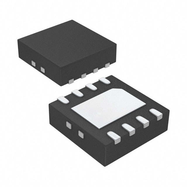
Package
The LT6100CDD#PBF comes in a compact dual die package (DD) that facilitates easy integration into circuit boards.
Essence
The essence of the LT6100CDD#PBF lies in its ability to accurately amplify and condition signals, making it an essential component in various electronic applications.
Packaging/Quantity
This product is typically packaged in reels or tubes, with each reel or tube containing a specific quantity of LT6100CDD#PBF ICs.
Specifications
- Supply Voltage Range: 2.7V to 36V
- Input Offset Voltage: ±100μV
- Gain Bandwidth Product: 10MHz
- Input Bias Current: ±20nA
- Operating Temperature Range: -40°C to 85°C
Detailed Pin Configuration
The LT6100CDD#PBF features a total of 8 pins, each serving a specific function:
- IN+ (Pin 1): Non-inverting input terminal
- IN- (Pin 2): Inverting input terminal
- V- (Pin 3): Negative power supply terminal
- OUT (Pin 4): Output terminal
- V+ (Pin 5): Positive power supply terminal
- REF (Pin 6): Reference voltage input terminal
- NC (Pin 7): No connection
- NC (Pin 8): No connection
Functional Features
- Differential Amplification: The LT6100CDD#PBF amplifies the difference between the IN+ and IN- inputs.
- Common Mode Rejection: It effectively rejects common-mode signals, allowing for accurate amplification of differential signals.
- Voltage Reference Input: The REF pin allows for precise control of the output voltage level.
Advantages and Disadvantages
Advantages
- High precision amplification
- Low noise figure
- Wide bandwidth for signal processing
- Low power consumption
Disadvantages
- Limited operating temperature range (-40°C to 85°C)
- Requires external voltage reference for optimal performance
Working Principles
The LT6100CDD#PBF operates based on the principles of differential amplification. It amplifies the voltage difference between the non-inverting (IN+) and inverting (IN-) input terminals while rejecting common-mode signals. This allows for accurate amplification and conditioning of differential signals.
Detailed Application Field Plans
The LT6100CDD#PBF finds applications in various fields, including: 1. Industrial automation: Signal conditioning in control systems and sensors. 2. Medical devices: Amplification and filtering of biomedical signals. 3. Communication systems: Signal conditioning for data transmission and reception. 4. Test and measurement equipment: Precise signal amplification and conditioning for accurate measurements.
Detailed and Complete Alternative Models
- LT6100IDD#PBF: Similar to LT6100CDD#PBF but comes in an alternative package (IDD).
- LT6100CMS8#PBF: Surface mount version of LT6100CDD#PBF in a smaller package (MS8).
- LT6100HMS8#PBF: High temperature variant of LT6100CMS8#PBF, suitable for extended temperature range applications.
(Note: This is not an exhaustive list; there are other alternative models available from the manufacturer.)
In conclusion, the LT6100CDD#PBF is a high-precision integrated circuit used for signal amplification and conditioning. Its low noise, wide bandwidth, and low power consumption make it suitable for various applications in different fields. However, it has limitations in terms of operating temperature range and requires an external voltage reference for optimal performance. Alternative models with different packages and specifications are also available to suit specific requirements.
Liste 10 perguntas e respostas comuns relacionadas à aplicação de LT6100CDD#PBF em soluções técnicas
Sure! Here are 10 common questions and answers related to the application of LT6100CDD#PBF in technical solutions:
Q: What is LT6100CDD#PBF? A: LT6100CDD#PBF is a precision instrumentation amplifier designed for low voltage applications.
Q: What is the input voltage range of LT6100CDD#PBF? A: The input voltage range of LT6100CDD#PBF is typically ±250mV.
Q: What is the gain accuracy of LT6100CDD#PBF? A: The gain accuracy of LT6100CDD#PBF is typically 0.05%.
Q: Can LT6100CDD#PBF operate on a single supply voltage? A: Yes, LT6100CDD#PBF can operate on a single supply voltage ranging from 2.7V to 36V.
Q: What is the bandwidth of LT6100CDD#PBF? A: The bandwidth of LT6100CDD#PBF is typically 1MHz.
Q: Is LT6100CDD#PBF suitable for low power applications? A: Yes, LT6100CDD#PBF has a low quiescent current of typically 60µA, making it suitable for low power applications.
Q: Can LT6100CDD#PBF handle high common-mode voltages? A: Yes, LT6100CDD#PBF can handle common-mode voltages up to ±275mV.
Q: Does LT6100CDD#PBF have built-in protection features? A: Yes, LT6100CDD#PBF has built-in protection against overvoltage and reverse supply conditions.
Q: What is the temperature range of LT6100CDD#PBF? A: LT6100CDD#PBF can operate in a temperature range of -40°C to 125°C.
Q: What are some typical applications of LT6100CDD#PBF? A: LT6100CDD#PBF is commonly used in precision measurement systems, industrial control systems, medical equipment, and data acquisition systems.
Please note that the answers provided here are general and may vary depending on specific datasheet specifications and application requirements.