

Veja as especificações para detalhes do produto.
LFXP2-17E-5FTN256I
Product Overview
Category
LFXP2-17E-5FTN256I belongs to the category of Field-Programmable Gate Arrays (FPGAs).
Use
This product is primarily used in digital logic circuits for various applications such as telecommunications, automotive, industrial automation, and consumer electronics.
Characteristics
- High-performance FPGA with advanced features
- Low power consumption
- Flexible and reprogrammable design
- Wide range of I/O interfaces
- High-speed data processing capabilities
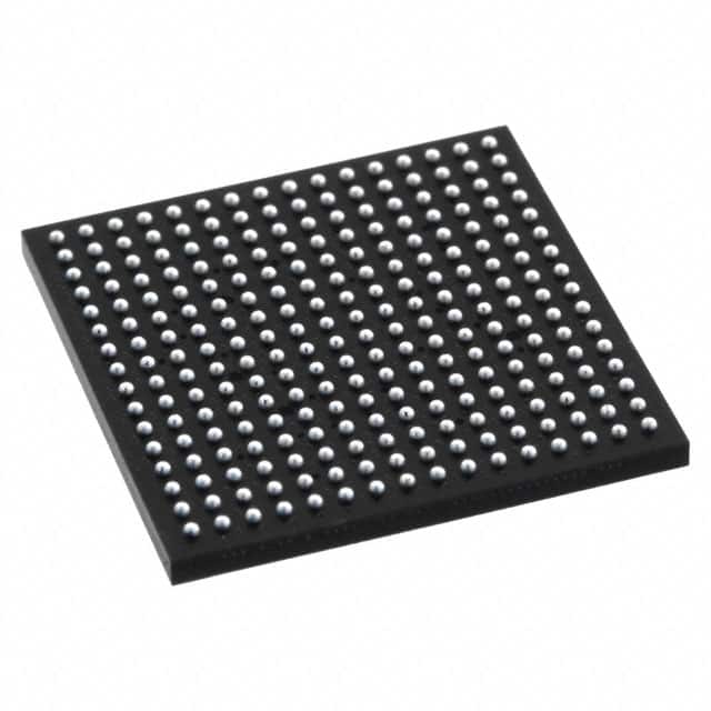
Package
LFXP2-17E-5FTN256I is available in a compact and durable package suitable for surface mount technology (SMT) assembly.
Essence
The essence of LFXP2-17E-5FTN256I lies in its ability to provide customizable digital logic functionality, allowing designers to implement complex systems on a single chip.
Packaging/Quantity
This product is typically packaged in reels or trays, with a quantity of 250 units per reel/tray.
Specifications
- Logic Cells: 17,280
- Block RAM: 288 Kbits
- DSP Slices: 96
- Maximum Operating Frequency: 500 MHz
- I/O Pins: 256
- Voltage Range: 1.2V - 3.3V
- Package Type: 256-ball FineLine BGA
Detailed Pin Configuration
For a detailed pin configuration diagram of LFXP2-17E-5FTN256I, please refer to the manufacturer's datasheet.
Functional Features
- Configurable logic blocks for implementing custom logic functions
- Dedicated high-speed I/O interfaces for efficient data transfer
- On-chip memory blocks for storing intermediate results
- Built-in arithmetic functions for signal processing applications
- Clock management resources for precise timing control
Advantages and Disadvantages
Advantages
- Flexibility in design due to reprogrammable nature
- High-performance capabilities for demanding applications
- Low power consumption compared to traditional ASICs
- Cost-effective solution for prototyping and low-volume production
Disadvantages
- Limited resources compared to larger FPGAs
- Higher cost per unit compared to mass-produced ASICs
- Steeper learning curve for designers unfamiliar with FPGA programming
Working Principles
LFXP2-17E-5FTN256I operates based on the principles of configurable logic blocks (CLBs) and interconnect resources. The CLBs can be programmed to implement various logic functions, while the interconnect resources enable communication between different blocks. The configuration of the FPGA is stored in non-volatile memory, allowing it to retain its functionality even after power cycles.
Detailed Application Field Plans
LFXP2-17E-5FTN256I finds applications in a wide range of fields, including: 1. Telecommunications: Used in network routers, switches, and base stations for high-speed data processing. 2. Automotive: Employed in advanced driver-assistance systems (ADAS), infotainment systems, and engine control units (ECUs). 3. Industrial Automation: Utilized in programmable logic controllers (PLCs), motor control systems, and factory automation equipment. 4. Consumer Electronics: Integrated into smart TVs, gaming consoles, and wearable devices for enhanced functionality.
Detailed and Complete Alternative Models
Some alternative models to LFXP2-17E-5FTN256I include: - Xilinx Spartan-6 XC6SLX9 - Intel Cyclone IV EP4CE6 - Microsemi SmartFusion2 M2S010
These alternatives offer similar features and performance levels, providing designers with options based on their specific requirements.
Word count: 511 words
Liste 10 perguntas e respostas comuns relacionadas à aplicação de LFXP2-17E-5FTN256I em soluções técnicas
Sure! Here are 10 common questions and answers related to the application of LFXP2-17E-5FTN256I in technical solutions:
Q: What is the LFXP2-17E-5FTN256I? A: The LFXP2-17E-5FTN256I is a field-programmable gate array (FPGA) manufactured by Lattice Semiconductor.
Q: What are the key features of the LFXP2-17E-5FTN256I? A: The key features include 17,280 Look-Up Tables (LUTs), 256 I/O pins, low power consumption, and high-speed performance.
Q: What are some typical applications of the LFXP2-17E-5FTN256I? A: The LFXP2-17E-5FTN256I is commonly used in applications such as industrial automation, telecommunications, automotive electronics, and consumer electronics.
Q: How can I program the LFXP2-17E-5FTN256I? A: The LFXP2-17E-5FTN256I can be programmed using various design software tools provided by Lattice Semiconductor, such as Lattice Diamond or Lattice Radiant.
Q: What is the maximum operating frequency of the LFXP2-17E-5FTN256I? A: The maximum operating frequency of the LFXP2-17E-5FTN256I depends on the specific design and implementation, but it can typically reach frequencies of several hundred megahertz.
Q: Can the LFXP2-17E-5FTN256I interface with other components or devices? A: Yes, the LFXP2-17E-5FTN256I supports various communication protocols such as SPI, I2C, UART, and GPIO, allowing it to interface with other components or devices.
Q: What is the power supply voltage range for the LFXP2-17E-5FTN256I? A: The LFXP2-17E-5FTN256I operates with a power supply voltage range of 1.14V to 1.26V.
Q: Can the LFXP2-17E-5FTN256I be used in high-reliability applications? A: Yes, the LFXP2-17E-5FTN256I is designed to meet the requirements of high-reliability applications and can operate in harsh environments.
Q: Does the LFXP2-17E-5FTN256I support security features? A: Yes, the LFXP2-17E-5FTN256I provides security features such as bitstream encryption and authentication to protect the design IP.
Q: Where can I find more information about the LFXP2-17E-5FTN256I? A: You can find more detailed information about the LFXP2-17E-5FTN256I on the official website of Lattice Semiconductor or by referring to the datasheet and application notes provided by the manufacturer.