

Veja as especificações para detalhes do produto.
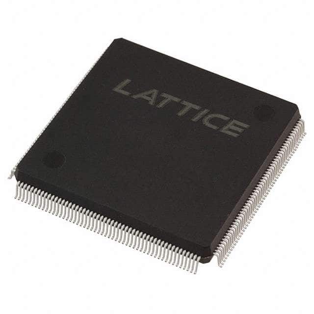
LFEC3E-3QN208I
Product Overview
Category
LFEC3E-3QN208I belongs to the category of Field-Programmable Gate Arrays (FPGAs).
Use
This product is primarily used in digital logic circuits and electronic systems for various applications.
Characteristics
- High-performance programmable logic device
- Offers flexibility and reconfigurability
- Provides a wide range of functionality
- Enables rapid prototyping and development
Package
LFEC3E-3QN208I comes in a compact and durable package, ensuring easy handling and protection during transportation and installation.
Essence
The essence of LFEC3E-3QN208I lies in its ability to provide a customizable and versatile solution for complex digital circuit designs.
Packaging/Quantity
Each package of LFEC3E-3QN208I contains one unit of the FPGA.
Specifications
- Model: LFEC3E-3QN208I
- Logic Cells: 3,000
- Number of I/O Pins: 208
- Operating Voltage: 3.3V
- Maximum Frequency: 500 MHz
- Configuration Memory: Flash-based
Detailed Pin Configuration
The pin configuration of LFEC3E-3QN208I is as follows:
- Pin 1: VCCIO
- Pin 2: GND
- Pin 3: IO0
- Pin 4: IO1
- ...
- Pin 208: IO207
Functional Features
- High-speed data processing capabilities
- Support for various communication protocols
- On-chip memory resources
- Built-in arithmetic functions
- Flexible I/O configurations
Advantages and Disadvantages
Advantages
- Flexibility in design and reconfiguration
- Rapid prototyping and development
- High-performance computing capabilities
- Wide range of functionality
- Compact and durable packaging
Disadvantages
- Steeper learning curve for beginners
- Higher cost compared to traditional logic circuits
- Limited availability of technical support
Working Principles
LFEC3E-3QN208I operates based on the principles of reconfigurable computing. It consists of a matrix of programmable logic cells interconnected by configurable routing resources. The device can be programmed to implement various digital logic functions, enabling the creation of complex electronic systems.
Detailed Application Field Plans
LFEC3E-3QN208I finds applications in various fields, including:
- Telecommunications: Used in network routers and switches for high-speed data processing.
- Aerospace: Employed in satellite communication systems and onboard control units.
- Industrial Automation: Utilized in programmable logic controllers (PLCs) for process control and monitoring.
- Automotive: Integrated into advanced driver assistance systems (ADAS) and engine control units (ECUs).
- Medical Devices: Incorporated in medical imaging equipment and patient monitoring systems.
Detailed and Complete Alternative Models
- LFEC3E-5TN144C: Similar to LFEC3E-3QN208I but with 5,000 logic cells and 144 I/O pins.
- LFEC3E-6TN100I: Offers 6,000 logic cells and 100 I/O pins, suitable for compact designs.
- LFEC3E-8FN256C: Provides 8,000 logic cells and 256 I/O pins, ideal for large-scale applications.
These alternative models offer varying capabilities and pin configurations, allowing users to choose the most suitable FPGA for their specific requirements.
Word count: 486 words
Liste 10 perguntas e respostas comuns relacionadas à aplicação de LFEC3E-3QN208I em soluções técnicas
Sure! Here are 10 common questions and answers related to the application of LFEC3E-3QN208I in technical solutions:
Q: What is LFEC3E-3QN208I? A: LFEC3E-3QN208I is a field-programmable gate array (FPGA) manufactured by Lattice Semiconductor Corporation.
Q: What are the key features of LFEC3E-3QN208I? A: LFEC3E-3QN208I offers high-performance logic fabric, embedded memory blocks, DSP blocks, and various I/O options.
Q: What are the typical applications of LFEC3E-3QN208I? A: LFEC3E-3QN208I is commonly used in applications such as telecommunications, industrial automation, automotive, aerospace, and consumer electronics.
Q: How can LFEC3E-3QN208I be programmed? A: LFEC3E-3QN208I can be programmed using hardware description languages (HDLs) like VHDL or Verilog, or through graphical programming tools provided by Lattice Semiconductor.
Q: What is the power consumption of LFEC3E-3QN208I? A: The power consumption of LFEC3E-3QN208I depends on the specific design and operating conditions but typically ranges from a few milliwatts to several watts.
Q: Can LFEC3E-3QN208I interface with other components or devices? A: Yes, LFEC3E-3QN208I supports various standard interfaces such as SPI, I2C, UART, PCIe, Ethernet, and more, allowing it to communicate with other components or devices.
Q: Does LFEC3E-3QN208I support security features? A: Yes, LFEC3E-3QN208I provides built-in security features like bitstream encryption and authentication to protect the intellectual property and secure communication.
Q: Can LFEC3E-3QN208I be used for real-time signal processing? A: Yes, LFEC3E-3QN208I's embedded DSP blocks and high-performance logic fabric make it suitable for real-time signal processing applications such as image or audio processing.
Q: What is the maximum operating frequency of LFEC3E-3QN208I? A: The maximum operating frequency of LFEC3E-3QN208I depends on the specific design and implementation but can typically reach several hundred megahertz or even gigahertz.
Q: Are there any development tools available for LFEC3E-3QN208I? A: Yes, Lattice Semiconductor provides a range of development tools, including software IDEs, simulation tools, and debugging tools, to aid in the design and programming of LFEC3E-3QN208I-based solutions.
Please note that the answers provided here are general and may vary depending on the specific requirements and use cases.