

Veja as especificações para detalhes do produto.
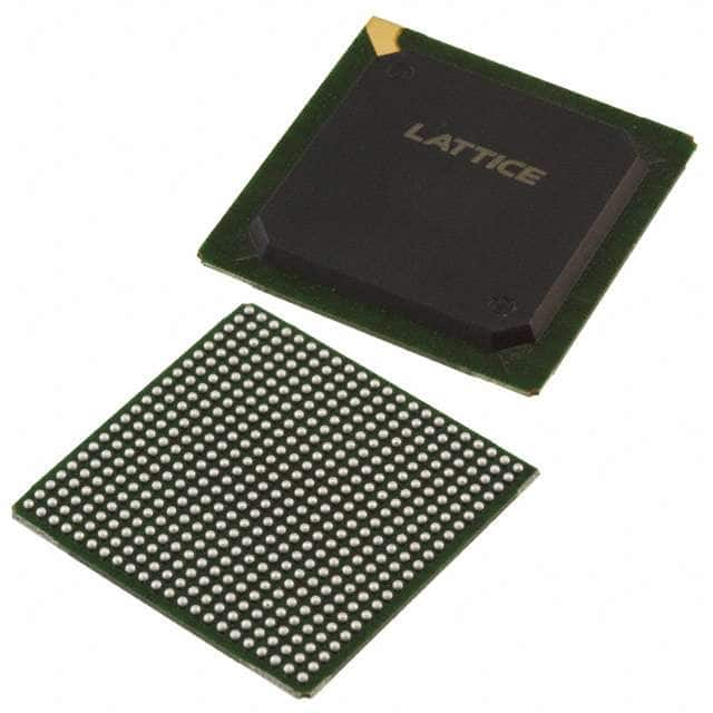
LFEC33E-4FN484C
Product Overview
Category
LFEC33E-4FN484C belongs to the category of Field Programmable Gate Arrays (FPGAs).
Use
This product is primarily used in digital logic circuits for various applications such as telecommunications, automotive, industrial automation, and consumer electronics.
Characteristics
- High-performance programmable logic device
- Low power consumption
- Flexible and reconfigurable design
- Large number of configurable logic blocks
- High-speed data processing capabilities
Package
LFEC33E-4FN484C is available in a 484-pin Fine-Pitch Ball Grid Array (FBGA) package.
Essence
The essence of LFEC33E-4FN484C lies in its ability to provide a customizable and efficient solution for complex digital circuit designs.
Packaging/Quantity
LFEC33E-4FN484C is typically packaged individually and is available in various quantities depending on the manufacturer's specifications.
Specifications
- Logic Elements: 33,280
- Flip-Flops: 66,560
- Block RAM: 1,152 Kbits
- Maximum Frequency: 500 MHz
- I/O Pins: 484
- Operating Voltage: 1.2V
Detailed Pin Configuration
The pin configuration of LFEC33E-4FN484C is as follows:
- Pin 1: VCCIO
- Pin 2: GND
- Pin 3: IOB33
- Pin 4: IOB32
- ...
- Pin 483: IOB2
- Pin 484: IOB1
Functional Features
- High-speed data processing capabilities
- Configurable I/O standards
- Embedded memory blocks for efficient data storage
- Dedicated clock management resources
- Support for various communication protocols
- On-chip debugging and testing features
Advantages and Disadvantages
Advantages
- Flexibility in design due to programmable nature
- High-performance capabilities for complex applications
- Low power consumption compared to traditional ASICs
- Cost-effective solution for prototyping and low-volume production
Disadvantages
- Limited scalability compared to custom-designed ASICs
- Higher cost per unit compared to mass-produced integrated circuits
- Longer development time compared to off-the-shelf solutions
Working Principles
LFEC33E-4FN484C operates based on the principles of reconfigurable logic. It consists of a large number of configurable logic blocks interconnected through programmable routing resources. The device can be programmed using Hardware Description Languages (HDL) such as VHDL or Verilog, allowing designers to define the desired functionality of the circuit.
Detailed Application Field Plans
LFEC33E-4FN484C finds applications in various fields, including:
- Telecommunications: Used in base stations, network routers, and communication infrastructure.
- Automotive: Employed in advanced driver assistance systems, engine control units, and infotainment systems.
- Industrial Automation: Utilized in programmable logic controllers, motor control systems, and factory automation equipment.
- Consumer Electronics: Integrated into high-definition televisions, gaming consoles, and multimedia devices.
Detailed and Complete Alternative Models
- LFEC33E-5FN484C: Similar to LFEC33E-4FN484C with enhanced performance and additional features.
- LFEC33E-6FN484C: Higher-density version of LFEC33E-4FN484C with increased logic elements and I/O pins.
- LFEC33E-4FN256C: Smaller package variant of LFEC33E-4FN484C with reduced pin count.
These alternative models provide options with varying specifications and packaging to cater to different design requirements.
In conclusion, LFEC33E-4FN484C is a high-performance FPGA that offers flexibility, efficiency, and reconfigurability for digital logic circuit designs. Its wide range of applications and availability of alternative models make it a versatile choice for various industries.
Liste 10 perguntas e respostas comuns relacionadas à aplicação de LFEC33E-4FN484C em soluções técnicas
Sure! Here are 10 common questions and answers related to the application of LFEC33E-4FN484C in technical solutions:
Q: What is LFEC33E-4FN484C? A: LFEC33E-4FN484C is a specific model of Field-Programmable Gate Array (FPGA) manufactured by Lattice Semiconductor.
Q: What are the key features of LFEC33E-4FN484C? A: LFEC33E-4FN484C offers 33,000 Look-Up Tables (LUTs), 1,620 kilobits of embedded memory, and 332 user I/O pins, among other features.
Q: In what applications can LFEC33E-4FN484C be used? A: LFEC33E-4FN484C can be used in various applications such as industrial automation, telecommunications, automotive electronics, and medical devices.
Q: How does LFEC33E-4FN484C differ from other FPGAs? A: LFEC33E-4FN484C stands out for its low power consumption, high performance, and small form factor, making it suitable for power-constrained applications.
Q: Can LFEC33E-4FN484C be programmed using industry-standard tools? A: Yes, LFEC33E-4FN484C can be programmed using popular design software like Lattice Diamond or Intel Quartus Prime.
Q: What are the voltage requirements for LFEC33E-4FN484C? A: LFEC33E-4FN484C operates at a core voltage of 1.2V and supports various I/O voltage standards, including 1.8V, 2.5V, and 3.3V.
Q: Can LFEC33E-4FN484C be used in safety-critical applications? A: Yes, LFEC33E-4FN484C is suitable for safety-critical applications as it offers built-in error detection and correction capabilities.
Q: Are there any development boards available for LFEC33E-4FN484C? A: Yes, Lattice Semiconductor provides development boards like the ECP5 Versa Evaluation Board that can be used with LFEC33E-4FN484C.
Q: Can LFEC33E-4FN484C be used in high-speed data processing applications? A: Absolutely, LFEC33E-4FN484C supports high-speed interfaces like DDR3/DDR4 memory controllers and PCIe, making it suitable for data-intensive applications.
Q: Where can I find more information about LFEC33E-4FN484C? A: You can visit the official website of Lattice Semiconductor or refer to the LFEC33E-4FN484C datasheet for detailed technical information.