

Veja as especificações para detalhes do produto.
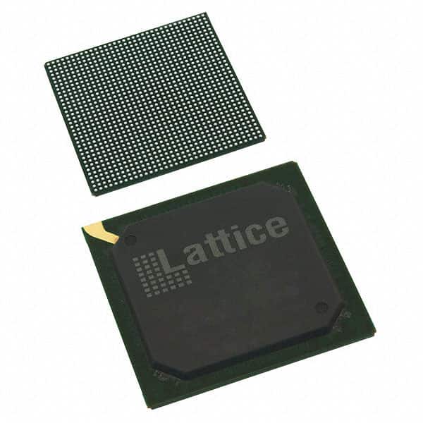
LFE3-70EA-7LFN1156I
Product Overview
Category
The LFE3-70EA-7LFN1156I belongs to the category of Field Programmable Gate Arrays (FPGAs).
Use
This FPGA is commonly used in electronic circuits for digital logic implementation and signal processing applications.
Characteristics
- High-performance programmable logic device
- Offers flexibility and reconfigurability
- Capable of implementing complex digital systems
- Provides high-speed data processing capabilities
Package
The LFE3-70EA-7LFN1156I comes in a compact package suitable for integration into various electronic devices.
Essence
The essence of this FPGA lies in its ability to provide a customizable and versatile solution for digital circuit design and implementation.
Packaging/Quantity
The LFE3-70EA-7LFN1156I is typically packaged individually and is available in various quantities depending on the manufacturer's specifications.
Specifications
- Logic Elements: 70,000
- Embedded Memory: 4.9 Mb
- DSP Blocks: 126
- Maximum User I/Os: 1,156
- Operating Voltage: 1.2V
- Speed Grade: 7
Detailed Pin Configuration
The LFE3-70EA-7LFN1156I has a comprehensive pin configuration that includes input/output pins, power supply pins, and configuration pins. The detailed pin configuration can be found in the product datasheet provided by the manufacturer.
Functional Features
- High-speed data processing capabilities
- Configurable logic elements for custom circuit implementation
- Embedded memory blocks for efficient data storage
- Digital Signal Processing (DSP) blocks for signal processing tasks
- Flexible I/O options for interfacing with external devices
Advantages and Disadvantages
Advantages
- Flexibility and reconfigurability for adapting to changing design requirements
- High-performance capabilities for complex digital system implementation
- Efficient use of resources with embedded memory and DSP blocks
Disadvantages
- Steep learning curve for beginners due to the complexity of FPGA programming
- Higher cost compared to other digital logic implementation alternatives
- Limited availability of alternative models with similar specifications
Working Principles
The LFE3-70EA-7LFN1156I operates based on the principles of configurable logic elements, which can be programmed to perform specific functions. These logic elements are interconnected through programmable routing resources, allowing for the creation of custom digital circuits. The FPGA's configuration is stored in non-volatile memory, enabling it to retain its programmed functionality even after power cycles.
Detailed Application Field Plans
The LFE3-70EA-7LFN1156I finds applications in various fields, including:
- Communications: Used in wireless communication systems for signal processing and protocol implementation.
- Industrial Automation: Employed in control systems for real-time data processing and interfacing with sensors and actuators.
- Aerospace and Defense: Utilized in radar systems, avionics, and military-grade communication equipment.
- Medical Devices: Integrated into medical imaging systems and diagnostic equipment for high-speed data processing.
- Automotive: Applied in advanced driver assistance systems (ADAS) and automotive infotainment systems.
Detailed and Complete Alternative Models
While the LFE3-70EA-7LFN1156I offers a comprehensive set of features, there are alternative FPGA models available in the market that cater to different design requirements. Some notable alternatives include:
- Xilinx Virtex UltraScale+: Offers higher logic capacity and performance for demanding applications.
- Intel Cyclone 10 GX: Provides a cost-effective solution with moderate performance and power efficiency.
- Microchip PolarFire: Focuses on low-power applications with high-security features.
These alternative models offer varying specifications and capabilities, allowing designers to choose the most suitable FPGA for their specific needs.
In conclusion, the LFE3-70EA-7LFN1156I is a high-performance FPGA that provides flexibility, reconfigurability, and efficient digital circuit implementation. Its wide range of applications and availability of alternative models make it a valuable component in various electronic systems.
Liste 10 perguntas e respostas comuns relacionadas à aplicação de LFE3-70EA-7LFN1156I em soluções técnicas
Sure! Here are 10 common questions and answers related to the application of LFE3-70EA-7LFN1156I in technical solutions:
Q: What is the LFE3-70EA-7LFN1156I? A: The LFE3-70EA-7LFN1156I is a field-programmable gate array (FPGA) manufactured by Lattice Semiconductor.
Q: What are the key features of the LFE3-70EA-7LFN1156I? A: The key features include 70,000 lookup tables (LUTs), high-speed I/O interfaces, embedded memory blocks, and low power consumption.
Q: What are some typical applications of the LFE3-70EA-7LFN1156I? A: The LFE3-70EA-7LFN1156I is commonly used in applications such as telecommunications, industrial automation, automotive electronics, and medical devices.
Q: How can I program the LFE3-70EA-7LFN1156I? A: The LFE3-70EA-7LFN1156I can be programmed using various design tools provided by Lattice Semiconductor, such as Lattice Diamond or Lattice Radiant.
Q: What is the maximum operating frequency of the LFE3-70EA-7LFN1156I? A: The maximum operating frequency depends on the specific design and implementation, but it can typically reach several hundred megahertz (MHz).
Q: Can the LFE3-70EA-7LFN1156I interface with other components or devices? A: Yes, the LFE3-70EA-7LFN1156I supports various I/O standards, including LVCMOS, LVTTL, LVDS, and differential signaling.
Q: Does the LFE3-70EA-7LFN1156I have any built-in memory? A: Yes, the LFE3-70EA-7LFN1156I has embedded memory blocks (RAM) that can be used for storing data within the FPGA.
Q: What is the power consumption of the LFE3-70EA-7LFN1156I? A: The power consumption depends on the specific design and utilization of the FPGA, but it is generally designed to be low power.
Q: Can the LFE3-70EA-7LFN1156I be reprogrammed multiple times? A: Yes, the LFE3-70EA-7LFN1156I is a reprogrammable FPGA, allowing for multiple programming cycles during development or in the field.
Q: Are there any development boards or evaluation kits available for the LFE3-70EA-7LFN1156I? A: Yes, Lattice Semiconductor provides development boards and evaluation kits specifically designed for the LFE3-70EA-7LFN1156I, which can aid in prototyping and testing.