

Veja as especificações para detalhes do produto.
LCMXO2280C-3FTN324C
Product Overview
Category
The LCMXO2280C-3FTN324C belongs to the category of Field Programmable Gate Arrays (FPGAs).
Use
This FPGA is commonly used in various electronic devices and systems for digital logic implementation, such as in telecommunications, automotive, industrial control, and consumer electronics.
Characteristics
- High-performance FPGA with low power consumption
- Compact size and high integration
- Flexible and reconfigurable design
- Support for complex digital logic functions
- Wide range of I/O interfaces
Package
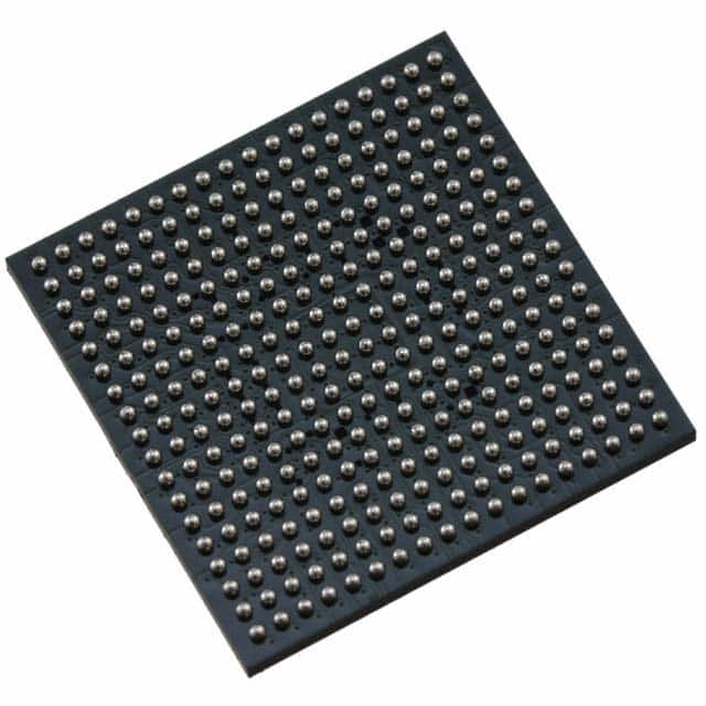
The LCMXO2280C-3FTN324C is available in a compact package, which ensures easy integration into electronic circuits. The package type is FTN324C.
Essence
The essence of the LCMXO2280C-3FTN324C lies in its ability to provide a customizable and programmable digital logic solution for various applications.
Packaging/Quantity
The LCMXO2280C-3FTN324C is typically packaged in reels or trays, depending on the manufacturer's specifications. The quantity per reel or tray may vary, but it is usually in the range of several hundred units.
Specifications
- Logic Elements: 2280
- Flip-Flops: 4560
- Block RAM: 270 Kb
- Maximum Frequency: 300 MHz
- I/O Pins: 324
- Voltage Range: 1.2V - 3.3V
- Operating Temperature: -40°C to 85°C
Detailed Pin Configuration
The LCMXO2280C-3FTN324C has a total of 324 pins, each serving a specific purpose in the FPGA's functionality. The pin configuration includes input/output pins, power supply pins, clock pins, and configuration pins. For a detailed pin configuration diagram, please refer to the manufacturer's datasheet.
Functional Features
- High-speed performance for demanding applications
- Low power consumption for energy-efficient designs
- Configurable I/O standards for compatibility with various interfaces
- On-chip memory blocks for efficient data storage
- Dedicated clock management resources for precise timing control
- Support for multiple design languages and development tools
Advantages and Disadvantages
Advantages
- Versatile and flexible design options
- Rapid prototyping and development cycles
- Cost-effective solution compared to custom ASICs
- Reconfigurable nature allows for design updates and modifications
- Wide range of available IP cores for accelerated development
Disadvantages
- Limited resources compared to dedicated ASICs
- Higher power consumption compared to specialized hardware
- Steeper learning curve for beginners in FPGA design
- Potential for design errors due to complex programming
Working Principles
The LCMXO2280C-3FTN324C operates based on the principles of digital logic implementation using programmable logic blocks, interconnects, and configurable routing resources. The FPGA can be programmed using Hardware Description Languages (HDL) such as VHDL or Verilog, which define the desired functionality of the digital circuit. Once programmed, the FPGA executes the specified logic operations, providing the desired output based on the input signals.
Detailed Application Field Plans
The LCMXO2280C-3FTN324C finds applications in various fields, including:
- Telecommunications: Used in network routers, switches, and base stations for high-speed data processing and protocol handling.
- Automotive: Employed in automotive electronics for engine control units, advanced driver-assistance systems, and infotainment systems.
- Industrial Control: Utilized in industrial automation systems for process control, monitoring, and communication between devices.
- Consumer Electronics: Integrated into smart TVs, gaming consoles, and home automation systems for enhanced functionality and connectivity.
Detailed and Complete Alternative Models
- LCMXO2560C-3FTN324C: Similar to LCMXO2280C-3FTN324C but with higher logic capacity.
- LCMXO640C-3FTN256C: Lower-cost alternative with reduced logic capacity.
- LCMXO1200C-3FTN256C: Higher-performance option with increased I/O pins.
These alternative models offer varying levels of performance, capacity, and cost to cater to different project requirements.
Word count: 550 words
Liste 10 perguntas e respostas comuns relacionadas à aplicação de LCMXO2280C-3FTN324C em soluções técnicas
Sure! Here are 10 common questions and answers related to the application of LCMXO2280C-3FTN324C in technical solutions:
Q: What is the LCMXO2280C-3FTN324C? A: The LCMXO2280C-3FTN324C is a low-cost, low-power FPGA (Field-Programmable Gate Array) device manufactured by Lattice Semiconductor.
Q: What are the key features of the LCMXO2280C-3FTN324C? A: The key features include 2280 Look-Up Tables (LUTs), 64Kbits of embedded memory, 32 multipliers, 4 PLLs (Phase-Locked Loops), and support for various I/O standards.
Q: What are some typical applications of the LCMXO2280C-3FTN324C? A: The LCMXO2280C-3FTN324C is commonly used in applications such as industrial automation, motor control, communication systems, medical devices, and consumer electronics.
Q: How can I program the LCMXO2280C-3FTN324C? A: The LCMXO2280C-3FTN324C can be programmed using Lattice Diamond or Lattice Radiant software tools, which provide a graphical interface for designing and programming the FPGA.
Q: What is the maximum operating frequency of the LCMXO2280C-3FTN324C? A: The maximum operating frequency of the LCMXO2280C-3FTN324C depends on the specific design and implementation, but it can typically reach frequencies up to 200 MHz.
Q: Can I interface the LCMXO2280C-3FTN324C with other devices? A: Yes, the LCMXO2280C-3FTN324C supports various I/O standards such as LVCMOS, LVTTL, and LVDS, allowing it to interface with a wide range of external devices.
Q: Is the LCMXO2280C-3FTN324C suitable for low-power applications? A: Yes, the LCMXO2280C-3FTN324C is designed to be low-power, making it suitable for battery-powered or energy-efficient applications.
Q: Can I reprogram the LCMXO2280C-3FTN324C after it has been programmed once? A: Yes, the LCMXO2280C-3FTN324C is a reprogrammable FPGA, allowing you to modify and reconfigure its functionality multiple times.
Q: Are there any development boards available for the LCMXO2280C-3FTN324C? A: Yes, Lattice Semiconductor provides development boards like the Lattice iCE40 UltraPlus Breakout Board, which can be used for prototyping and evaluation of the LCMXO2280C-3FTN324C.
Q: Where can I find more information about the LCMXO2280C-3FTN324C? A: You can find more detailed information, datasheets, application notes, and reference designs on the official website of Lattice Semiconductor or by contacting their technical support team.