

Veja as especificações para detalhes do produto.
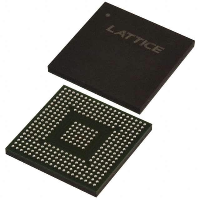
LCMXO2-4000ZE-2BG332C
Product Overview
Category
The LCMXO2-4000ZE-2BG332C belongs to the category of Field Programmable Gate Arrays (FPGAs).
Use
FPGAs are integrated circuits that can be programmed and reprogrammed to perform various digital functions. The LCMXO2-4000ZE-2BG332C is specifically designed for applications requiring low power consumption and high performance.
Characteristics
- Low power consumption: The LCMXO2-4000ZE-2BG332C is optimized for low power operation, making it suitable for battery-powered devices.
- High performance: With a high logic density and advanced architecture, this FPGA offers fast processing capabilities.
- Small package size: The LCMXO2-4000ZE-2BG332C comes in a compact package, making it ideal for space-constrained designs.
- Versatile I/O options: It provides a wide range of input/output options, allowing for flexible connectivity.
Package and Quantity
The LCMXO2-4000ZE-2BG332C is available in a Ball Grid Array (BGA) package. Each package contains one unit of the FPGA.
Specifications
- Logic Cells: 4000
- Look-Up Tables (LUTs): 4000
- Flip-Flops: 8000
- Block RAM: 112 Kbits
- Maximum Frequency: 100 MHz
- Operating Voltage: 1.2V
- I/O Voltage: 3.3V
- Package Type: BGA
- Package Pins: 332
Pin Configuration
The pin configuration of the LCMXO2-4000ZE-2BG332C FPGA is as follows:

Functional Features
- Programmable Logic: The FPGA offers a flexible programmable logic fabric that can be configured to implement various digital functions.
- I/O Interfaces: It provides multiple I/O interfaces, including GPIO, UART, SPI, and I2C, enabling easy integration with external devices.
- Clock Management: The FPGA includes built-in clock management resources, such as PLLs and DLLs, for precise timing control.
- Embedded Memory: With on-chip block RAM, the LCMXO2-4000ZE-2BG332C allows for efficient data storage and retrieval.
Advantages and Disadvantages
Advantages
- Low power consumption makes it suitable for battery-powered applications.
- High-performance capabilities enable fast processing of complex algorithms.
- Compact package size allows for space-efficient designs.
- Versatile I/O options provide flexibility in connectivity.
Disadvantages
- Limited logic cell count compared to higher-end FPGAs.
- Relatively smaller memory capacity may restrict certain applications.
- Availability of alternative models with different features may limit specific use cases.
Working Principles
The LCMXO2-4000ZE-2BG332C FPGA operates based on the principles of reconfigurable logic. It consists of an array of configurable logic blocks interconnected through programmable routing resources. The user can program the FPGA using Hardware Description Languages (HDL) to define the desired functionality. Upon configuration, the FPGA executes the programmed logic, allowing for the implementation of complex digital systems.
Application Field Plans
The LCMXO2-4000ZE-2BG332C FPGA finds applications in various fields, including:
- Embedded Systems: It can be used in embedded systems for controlling and interfacing with peripheral devices.
- Communications: The FPGA enables the implementation of communication protocols and signal processing algorithms.
- Industrial Automation: It can be utilized in industrial automation systems for real-time control and monitoring.
- Medical Devices: The FPGA can be integrated into medical devices for data acquisition, signal processing, and control functions.
Alternative Models
For users seeking alternative models with different specifications or features, the following FPGAs can be considered:
- LCMXO2-1200ZE-1TG144C
- LCMXO3LF-6900C-5BG484I
- LCMXO4L-640HC-4SG48C
These alternatives offer varying logic cell counts, I/O options, and package types to cater to specific application requirements.
In conclusion, the LCMXO2-4000ZE-2BG332C FPGA is a low-power, high-performance device that finds applications in diverse fields. Its compact size, versatile I/O options, and programmable logic make it a suitable choice for various digital designs.
Liste 10 perguntas e respostas comuns relacionadas à aplicação de LCMXO2-4000ZE-2BG332C em soluções técnicas
Sure! Here are 10 common questions and answers related to the application of LCMXO2-4000ZE-2BG332C in technical solutions:
Q: What is the LCMXO2-4000ZE-2BG332C? A: The LCMXO2-4000ZE-2BG332C is a low-cost, low-power FPGA (Field-Programmable Gate Array) device manufactured by Lattice Semiconductor.
Q: What are the key features of the LCMXO2-4000ZE-2BG332C? A: Some key features include 4000 Look-Up Tables (LUTs), 64 Kbits of embedded Block RAM, 58 user I/O pins, and support for various I/O standards.
Q: What are some typical applications of the LCMXO2-4000ZE-2BG332C? A: The LCMXO2-4000ZE-2BG332C is commonly used in applications such as industrial control systems, consumer electronics, communication devices, and automotive systems.
Q: How can I program the LCMXO2-4000ZE-2BG332C? A: The LCMXO2-4000ZE-2BG332C can be programmed using Lattice Diamond or Lattice Radiant software tools, which provide a graphical interface for designing and programming the FPGA.
Q: What voltage levels does the LCMXO2-4000ZE-2BG332C support? A: The LCMXO2-4000ZE-2BG332C supports both 3.3V and 1.2V voltage levels, allowing for compatibility with a wide range of peripherals and interfaces.
Q: Can I use the LCMXO2-4000ZE-2BG332C in battery-powered applications? A: Yes, the LCMXO2-4000ZE-2BG332C is designed to be power-efficient and can be used in battery-powered applications where low power consumption is critical.
Q: Does the LCMXO2-4000ZE-2BG332C support high-speed interfaces like USB or Ethernet? A: Yes, the LCMXO2-4000ZE-2BG332C supports various high-speed interfaces through its configurable I/O pins, making it suitable for applications requiring USB or Ethernet connectivity.
Q: Can I reprogram the LCMXO2-4000ZE-2BG332C multiple times? A: Yes, the LCMXO2-4000ZE-2BG332C is a reprogrammable FPGA, allowing you to modify and reconfigure the design multiple times as needed.
Q: Are there any development boards available for the LCMXO2-4000ZE-2BG332C? A: Yes, Lattice Semiconductor provides development boards specifically designed for the LCMXO2-4000ZE-2BG332C, which can help with prototyping and evaluation of your designs.
Q: Where can I find technical documentation and support for the LCMXO2-4000ZE-2BG332C? A: You can find technical documentation, datasheets, application notes, and support resources on the official website of Lattice Semiconductor or by contacting their customer support team.