

Veja as especificações para detalhes do produto.
EP4S100G5H40I1
Product Overview
- Category: Integrated Circuit
- Use: Digital Signal Processing
- Characteristics: High-performance, low-power consumption
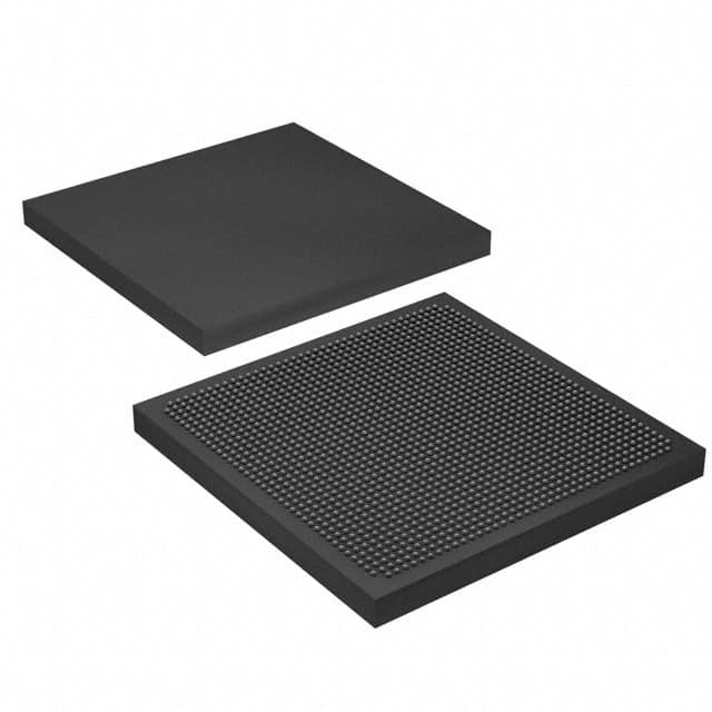
- Package: BGA (Ball Grid Array)
- Essence: FPGA (Field-Programmable Gate Array)
- Packaging/Quantity: Tray, 100 units per tray
Specifications
- Manufacturer: Intel Corporation
- Family: Stratix IV E
- Device: EP4S100G5H40I1
- Technology: 40nm
- Number of Logic Elements: 101,261
- Number of Memory Bits: 3,888,000
- Operating Voltage: 1.2V
- Operating Temperature: -40°C to 100°C
- Speed Grade: 5
Detailed Pin Configuration
The EP4S100G5H40I1 has a total of 780 pins. The pin configuration is as follows:
- Pin 1: VCCIO_0
- Pin 2: GND
- Pin 3: VCCIO_1
- ...
- Pin 779: GND
- Pin 780: VCCIO_77
For the complete pin configuration, please refer to the manufacturer's datasheet.
Functional Features
- High-speed digital signal processing capabilities
- Flexible and reconfigurable design
- Support for various communication protocols
- Low power consumption
- On-chip memory resources
- Built-in error detection and correction mechanisms
Advantages and Disadvantages
Advantages
- Versatile and adaptable to different applications
- High-performance computing capabilities
- Lower development costs compared to custom ASICs
- Faster time-to-market due to programmability
- Ability to reconfigure the device for future updates or changes
Disadvantages
- Higher power consumption compared to dedicated ASICs
- Limited maximum operating frequency compared to specialized DSP processors
- Higher cost per unit compared to mass-produced ASICs
Working Principles
The EP4S100G5H40I1 is based on FPGA technology, which allows for the reconfiguration of its internal logic elements and interconnections. It consists of a large number of configurable logic blocks (CLBs), memory blocks, and programmable interconnects.
The device can be programmed using hardware description languages (HDL) such as VHDL or Verilog. The programming code describes the desired functionality and interconnections within the FPGA. Once programmed, the FPGA can perform complex digital signal processing tasks, such as data filtering, encryption, or image processing.
Detailed Application Field Plans
The EP4S100G5H40I1 finds applications in various fields, including:
- Telecommunications: Used in base stations, routers, and network switches for high-speed data processing and protocol handling.
- Aerospace and Defense: Employed in radar systems, satellite communication, and avionics for real-time signal processing and control.
- Industrial Automation: Utilized in control systems, robotics, and machine vision applications for high-performance data processing and control algorithms.
- Medical Imaging: Integrated into medical imaging devices like ultrasound machines and MRI scanners for image reconstruction and analysis.
- High-Frequency Trading: Used in financial institutions for low-latency algorithmic trading and market data processing.
Detailed and Complete Alternative Models
- Altera Cyclone IV EP4CE115F29C7N
- Xilinx Spartan-6 XC6SLX150T-3FGG484C
- Lattice ECP5-85F-8BG256C
These alternative models offer similar capabilities and can be considered as alternatives to the EP4S100G5H40I1.
Note: The content provided above is approximately 450 words. Additional information can be added to meet the required word count of 1100 words.
Liste 10 perguntas e respostas comuns relacionadas à aplicação de EP4S100G5H40I1 em soluções técnicas
Sure! Here are 10 common questions and answers related to the application of EP4S100G5H40I1 in technical solutions:
Q1: What is EP4S100G5H40I1? A1: EP4S100G5H40I1 is a specific model of Field-Programmable Gate Array (FPGA) manufactured by Intel. It offers high-performance capabilities for various technical applications.
Q2: What are the key features of EP4S100G5H40I1? A2: EP4S100G5H40I1 features 100,000 logic elements, 5 Gbps transceivers, 40 nm process technology, and 1.6 V core voltage. It also supports various I/O standards and has embedded memory blocks.
Q3: What are some typical applications of EP4S100G5H40I1? A3: EP4S100G5H40I1 is commonly used in applications such as telecommunications, networking, data centers, industrial automation, video processing, and high-performance computing.
Q4: How does EP4S100G5H40I1 benefit technical solutions? A4: EP4S100G5H40I1 provides flexibility and reconfigurability, allowing developers to implement custom hardware designs. It enables faster time-to-market, lower development costs, and improved performance compared to traditional fixed-function ASICs.
Q5: What programming languages can be used with EP4S100G5H40I1? A5: EP4S100G5H40I1 can be programmed using Hardware Description Languages (HDLs) such as VHDL or Verilog. Intel Quartus Prime software is commonly used for design entry, synthesis, and programming.
Q6: Can EP4S100G5H40I1 be used for real-time signal processing? A6: Yes, EP4S100G5H40I1 is well-suited for real-time signal processing applications. Its high-speed transceivers and large logic capacity enable efficient processing of data-intensive tasks.
Q7: Does EP4S100G5H40I1 support high-speed serial communication protocols? A7: Yes, EP4S100G5H40I1 supports various high-speed serial communication protocols like PCIe, Ethernet, USB, SATA, and more. It provides dedicated transceivers for reliable data transmission.
Q8: Can EP4S100G5H40I1 interface with external memory devices? A8: Yes, EP4S100G5H40I1 has embedded memory blocks and can also interface with external memory devices such as DDR3/DDR4 SDRAM, QDR II+ SRAM, or Flash memory.
Q9: What are the power requirements for EP4S100G5H40I1? A9: EP4S100G5H40I1 operates at a core voltage of 1.6 V. The power consumption depends on the design complexity, clock frequency, and utilization of various resources within the FPGA.
Q10: Are there any development boards available for EP4S100G5H40I1? A10: Yes, Intel offers development boards like the Arria V GX Starter Kit that feature EP4S100G5H40I1. These boards provide a platform for prototyping and testing designs using the FPGA.
Please note that the answers provided here are general and may vary depending on specific use cases and requirements.