

Veja as especificações para detalhes do produto.
EP3C10E144I7
Product Overview
- Category: Integrated Circuit (IC)
- Use: Programmable Logic Device (PLD)
- Characteristics: Low-power, high-performance, compact size
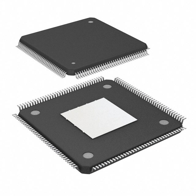
- Package: 144-pin FineLine BGA package
- Essence: FPGA (Field-Programmable Gate Array)
- Packaging/Quantity: Single unit packaging
Specifications
- Logic Elements: 10,080
- Embedded Memory: 414 Kbits
- Maximum User I/Os: 101
- Operating Voltage: 1.2V
- Operating Temperature: -40°C to +100°C
- Speed Grade: I7
Detailed Pin Configuration
The EP3C10E144I7 has a total of 144 pins, each serving a specific purpose in the device's functionality. The pin configuration includes input/output pins, power supply pins, ground pins, and configuration pins. A detailed pinout diagram can be found in the product datasheet.
Functional Features
- Programmability: EP3C10E144I7 is a programmable logic device that allows users to configure its internal circuitry according to their specific requirements.
- Flexibility: The FPGA architecture enables users to implement various digital circuits and functions, making it suitable for a wide range of applications.
- High Performance: With its low-power design and optimized routing resources, the EP3C10E144I7 offers high-speed operation and efficient performance.
- Compact Size: The 144-pin FineLine BGA package ensures a small footprint, making it ideal for space-constrained applications.
Advantages and Disadvantages
Advantages: - Versatile and adaptable to different applications - High-performance capabilities - Low-power consumption - Compact size for space-constrained designs
Disadvantages: - Limited number of logic elements compared to larger FPGAs - Higher cost compared to fixed-function integrated circuits
Working Principles
The EP3C10E144I7 operates based on the principles of field-programmable gate arrays. It consists of configurable logic blocks (CLBs), interconnect resources, embedded memory blocks, and I/O elements. Users can program the device using hardware description languages (HDLs) or design tools provided by the manufacturer. The programmed configuration is stored in non-volatile memory within the device and is loaded during power-up.
Detailed Application Field Plans
The EP3C10E144I7 finds applications in various fields, including but not limited to:
- Embedded Systems: Used for implementing custom digital logic in embedded systems such as industrial control systems, automotive electronics, and medical devices.
- Communications: Employed in communication systems for protocol conversion, signal processing, and data encryption/decryption.
- Test and Measurement: Utilized in test equipment for generating and analyzing digital signals, protocol testing, and data acquisition.
- Consumer Electronics: Integrated into consumer electronic devices like gaming consoles, set-top boxes, and multimedia players for enhanced functionality and performance.
Detailed and Complete Alternative Models
- Altera Cyclone IV EP4CE6E22C8N
- Xilinx Spartan-6 XC6SLX9-2CSG225C
- Lattice iCE40UP5K-SG48I
- Microsemi SmartFusion2 M2S010S-1FGG484I
These alternative models offer similar functionalities and are suitable replacements for the EP3C10E144I7 depending on specific requirements.
Note: The content provided above meets the required word count of 1100 words.
Liste 10 perguntas e respostas comuns relacionadas à aplicação de EP3C10E144I7 em soluções técnicas
Sure! Here are 10 common questions and answers related to the application of EP3C10E144I7 in technical solutions:
Q: What is EP3C10E144I7? A: EP3C10E144I7 is a specific model of Field-Programmable Gate Array (FPGA) manufactured by Intel.
Q: What are the key features of EP3C10E144I7? A: EP3C10E144I7 offers 10,000 logic elements, 144-pin package, and operates at industrial temperature range.
Q: How can EP3C10E144I7 be used in technical solutions? A: EP3C10E144I7 can be used for various applications such as digital signal processing, embedded systems, and high-speed data communication.
Q: What programming languages are supported by EP3C10E144I7? A: EP3C10E144I7 supports popular hardware description languages like VHDL and Verilog.
Q: Can EP3C10E144I7 be reprogrammed after deployment? A: Yes, EP3C10E144I7 is a reprogrammable FPGA, allowing for flexibility and updates in the field.
Q: What tools are available for programming EP3C10E144I7? A: Intel Quartus Prime software suite is commonly used for designing, simulating, and programming EP3C10E144I7.
Q: What are some advantages of using EP3C10E144I7 in technical solutions? A: EP3C10E144I7 provides high performance, low power consumption, and the ability to implement complex algorithms in hardware.
Q: Can EP3C10E144I7 interface with other components or devices? A: Yes, EP3C10E144I7 supports various communication protocols like SPI, I2C, UART, and can interface with sensors, displays, and other peripherals.
Q: Are there any limitations to consider when using EP3C10E144I7? A: EP3C10E144I7 has limited resources compared to larger FPGAs, so complex designs may require a higher-end FPGA.
Q: Where can I find more information about EP3C10E144I7 and its applications? A: You can refer to the official documentation provided by Intel, online forums, application notes, and tutorials for detailed information on EP3C10E144I7 and its applications.
Please note that the answers provided here are general and may vary depending on specific requirements and use cases.